Let me begin by saying I am not a programmer, my background mainly being digital and analog electronics - hardware rather than software. So the programs here really are home brew creations and mainly written for the purpose of troubleshooting arcade PCB hardware.
I've mentioned most of these test programs before in various PCB repair logs but as they share a common goal it seems worthwhile to gather them onto a single page.
Many arcade titles have inbuilt diagnostic routines which run upon startup or when a 'test' input is selected. But many, especially earlier or lesser known games have none. And what to do when a hardware fault prevents existing on board diagnostics from running?
That's when we reach for the test equipment be it logic probe, oscilloscope or if we are especially well equipped we may have a made for purpose tester such as the Fluke 9010A which connects to the PCB via the CPU socket (using a CPU specific test pod) and can perform various tests on the system resources from the CPU's point of view.
Sadly I don't have the funds (or the bench space) for a dedicated system tester and rely upon my analog oscilloscope for most fault tracing but it occurred to me that we could write some simple firmware and enlist the PCBs own CPU to assist with some of the troubleshooting tasks.
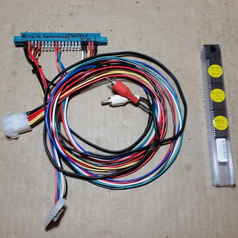
That was the case in this first example which I wrote to assist with a PCB repair; Missile Command by Atari. The game would not run, when test mode was selected the on board RAM test would complete (after I duly replaced one faulty 4116 RAM IC) but before the remaining diagnostic tests could run the program would freeze and the watchdog timer reset the 6502 CPU.
Although the RAM was now known to be good and I had already removed and verified the program ROMs, some other hardware issue was preventing the program from proceeding. Using the oscilloscope to trace the signals on board did not reveal anything as the program would fail too quickly to observe much activity.
Missile Command test cable and test EPROMs, 2020
My answer to this problem was the 'reading every address' loop. That program did little more than read every address from 0000 to 7fff in a continuous loop. It did nothing with the data read, what it did achieve was to create some predictable activity on the CPU address bus which could be viewed on an oscilloscope enabling hardware faults to be easily traced.
With the aid of the program loop I soon identified the address decoder issue affecting one half of one 2k Byte ROM and replaced the faulty component. With the PCB now running and on board diagnostics working correctly, at the time there was no need to develop the 'reading every address' program beyond that purpose.
I may revisit this program at a later date and add some testing routines which are not included in Atari's on board diagnostics such as the multiplexed RAM addressing modes. Meanwhile the 'reading every address' loop proved so successful for fault tracing I have incorporated that into my subsequent test ROM programs.
My next attempt at a test ROM, for the z80 CPU in Exerion by Jaleco was more ambitious. Exerion included no diagnostic software so I wrote a test routine which checked three areas of RAM, outputting results to that PCBs text layer, followed by a version of the 'reading every address' loop for good measure which also placed a character on screen for every address read to indicate continuing activity.
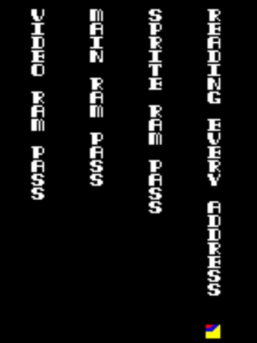
Exerion Test ROM, 2021 - running in MAME
Apart from filling every RAM address with each data value from 00 to FF Hex and reading those back the program could also identify addressing issues where data might be written to an incorrect address location and potentially overwritten by other data written to the same address.
To test for this type of issue the address of each RAM location is written as data and once complete each RAM address read back and its data compared to the address. As each 16 bit address amounts to two bytes of information the routine involves two passes, first for the high order address byte then for the lower.
For the Sprite RAM address testing I also wrote a rudimentary error display routine to assist with troubleshooting an issue where the tests would Pass when run in MAME but not on actual hardware. It turned out although the Sprite RAM comprises 1k Byte ( 2 x 2114 1k x 4 bit ICs) on the actual game PCB their upper 3 address inputs are tied to ground so only 128 Bytes of Sprite RAM are actually available.
I've since updated the RAM testing routines to only check those 128 bytes of Sprite RAM which are useable on the actual game PCB, the remaining bytes not used and impossible to access as configured in hardware.
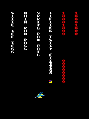
In the photo above with the test program running in MAME I've manually triggered the error display which shows the Sprite RAM address in question (in binary, reading from top to bottom) as 8800 Hex and next to that the data read back which in this case corresponds to the upper address byte 88. When running on actual hardware an error condition would be detected and displayed if the address and data values do not match at any point in the Sprite RAM Address testing routine.
Asm316.asm RAM Test Rev.6 Assembly listing
Prom5_diags6.4p RAM Test Rev.6 Hex file
For Shuttle Invader which is an earlier game using an 8080 CPU with a limited instruction set and only bitmap graphics ability achieving the same goal was more challenging. Compared to the z80 instruction set, the 8080 has no extended instructions for data fill or individual bit operations. The original EPROMs on the Shuttle Invader PCB are 2708s with only 1kByte of storage so the entire program including any graphics should ideally be written to fit within a single EPROM.
For a RAM testing program there is another limitation, the RAM itself can not be relied upon for the program to run. The entire program should only make use of the CPUs internal registers and the 'boot ROM' location for the program itself. That means no subroutines can be called or any data pushed onto the stack for temporary storage as these operations require a known good area of RAM to be set aside.
The program I've written begins by filling the dynamic RAM area with data, beginning with all zeros then reading each address back and checking for errors. If all good it increments the data and repeats the process for every data value from 00 to FF. As most of the DRAM is video memory the resulting patterns should be visible on screen as the test progresses. At the beginning of each test loop a brief, low pitch tone should also be heard.
If that completes correctly it does two more passes where the address of each memory location is written as data, first using the low order address byte of each memory location then the high order byte. The purpose of this last step is to identify any addressing errors where data may be written to the wrong memory location then overwritten by other data. If there are no errors a 'DRAM: PASS." graphic message is transferred to the video memory and a similar process commences for the static RAM area.
As the static RAM is being read, each byte read is also written to an area within the video RAM so the patterns read back from static RAM can be viewed on screen. If these tests pass a "SRAM: PASS." graphic message displays that result and the program moves on to a continuous 'reading every address' loop, also writing the data read to an area within the video memory so the activity can be viewed on screen.
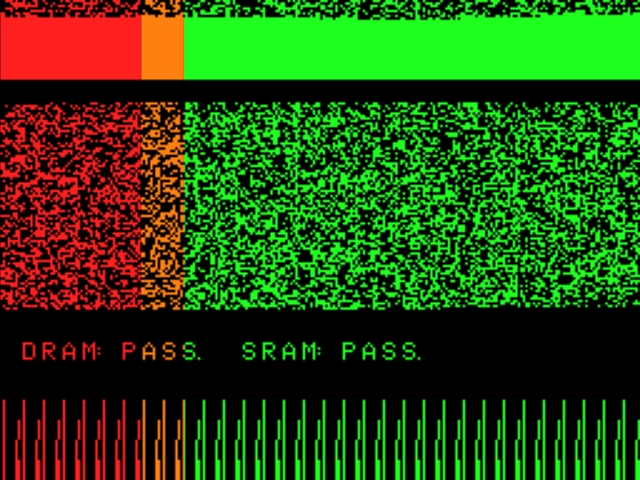
Shuttle Invader Test ROM, 2024 - running in MAME
At any point during the RAM testing if there is a read error a high pitch tone sounds and the program continuously rewrites and re reads that memory location, announcing the result with a low or high pitch tone each time. Repeating the write and read of that particular memory address allows the problem area to be identified in circuit using an oscilloscope or logic probe. In the latest version of the test ROM the address, data written and data read back from that location are decoded and displayed on screen as a graphic message allowing a faulty RAM IC to be identified directly.
Here is the Shuttle Invader Test ROM running in MAME; once again I've manually triggered the error display message where A is the address, D is the data written and R is the data read back. When testing actual hardware an error will be indicated if D and R are not equal.
Asm406.asm Shuttle Invader Test ROM v1.6 Assembly listing
test.13c Shuttle Invader Test ROM v1.6 Hex file
Having completed the test program for Shuttle Invader and proving its worth in a recent PCB repair it occurred to me the test routines contained within could be ported to other games of the era which employed similar hardware and had no existing diagnostic software available. The first example which came to mind was Space Fever by Nintendo.
To date I've managed to repair a number of Space Fever PCB sets without the aid of any diagnostics but may have saved a lot of time and guesswork if RAM faults could have been easily identified or eliminated. Of course the memory map and screen layout are different for the two games, requiring some parameter changes to the test program.
Although Space Fever has more RAM memory than Shuttle Invader the testing procedure is much simpler with just a single 16k bank of dynamic RAM for Space fever compared to Shuttle Invader's 8k dynamic plus 1k Byte of static RAM. That eliminates the need for a second set of RAM test routines, leaving some free space in the 1k Byte EPROM capacity so I decided to try my hand at adding a test routine for the shifter circuit in the Space Fever Hardware.
Space Fever Test ROM, 2024 - running on actual game PCB set
Many invader style games use a shifter circuit to quickly move the objects on screen by 1 - 7 pixels before they advance to the next byte of video RAM and the process then repeats. The shifter circuit is really just moving the graphics data within each byte to achieve fast scrolling rather than keeping track of the objects outright positions.
This saves processing time compared to performing the shift operations within the CPU and avoids an issue where shifting an object by multiple bits would take additional clock cycles for each extra bit shift operation.
Writing a test routine for the shifter circuit in Space Fever was a learning experience as it required a deeper understanding of the circuit to predict the correct operation and identify a fault situation. To begin with, a byte of data to be shifted is sent to a latch on the video PCB. Another latch is sent the shift value, from 0 to 7.
The data latch has two stages, the second stage will contain the byte of data which was latched in the previous shift operation. Using these two data bytes allows bits which would have overflowed from the previous shift operation to be effectively shifted into the current byte, providing a 'seamless' transition of objects as they are shifted pixel by pixel from one byte of screen RAM to the next.
For the purposes of testing, I found that a single data byte could be sent to the latch twice in succession so both stages would contain the same byte value. When the shifted value is read the bits within that byte should effectively be rotated; that is bits which overflow from bit 7 appear on bit 0.
So the test routine involves latching a byte of data (twice) with an initial shift amount of 0 and reading that back from the output of the shifter circuit. Then the shift amount is incremented, also a CPU 'rotate left' instruction is performed on the initial data so the data read back from the shifter can be compared with the predicted value.
If that is correct the process repeats for each shift value from 0 to 7 and each data value from 00 to ff. Of course if the initial data is 00 then the shifted value should always be 00 as well but every data and shift value is tested nonetheless. Should there be a discrepancy between the predicted and actual values read an error is displayed.
Space Fever Test ROM, 2024 - running in MAME
For the Space Fever test ROM, if there is an error with either the RAM or the shifter circuit the program will display an error code and then just retest the same error location repeatedly. If the error is intermittent the result will sound a 'pass' or 'fail' tone and update the display each time the same location is re tested.
For the RAM test the error message looks like Axxxx Dxx Rxx where A is the address, D is the data written and R is the data read back. If D and R are not the same there is an error.
If you see the DRAM: PASS. message and SHIFT: then an error code that is a shifter error where: A - the first two digits are the data sent to the shifter from 00 to FF and the next two digits are the shift amount from 00 to 07
D - is the calculated result using the CPU to do the shift operation and R - is the result read back from the shifter circuit. Once again, if D and R are not the same there is an error.
Asm615.asm Space fever Test ROM v1.5 Assembly listing
f1-test.bin Space fever Test ROM v1.5 Hex file
By the way, just the character graphics data for the pass / fail messages and numerals 0 to 9, letters A to F take up 256 bytes of the available 1024 so the program itself fits into the remaining 768 bytes of EPROM space. As mentioned the program should run even if the RAM is not working however a meaningful on screen display would require the video area of RAM to be working to some extent.
Even if the on screen display is garbled or the RAM completely corrupted the program should still function and output some sounds (if the sound is working). At the very least the test program should generate some repetitive activity in the area of the circuit where errors are present.
Just a little addition to my Homebrew test ROMs; here was a PCB mod and ROM hack to create a standalone RAM tester for 2114, 1k x 4 bit static RAM ICs.
These RAM chips are commonly used on arcade PCBs as well as early computers. I recently bought a batch of them online to upgrade the RAM on my Ohio Superboard II computer reproduction from 4k Bytes to a full complement of 8k Bytes, requiring another 8 ICs.
As usual the ICs received were obviously second hand reclaimed parts which had been scrubbed off and re marked, having identical part number and date code markings despite being in different packages with slight variations in the plastic mouldings such as the shape of the slot which identifies pin 1. Some still had different manufacturer codes printed on the underside of the DIP package.
That's pretty much par for the course with these obsolete components so the real challenge is to see if any or all of these components actually work. Initial results, plugging the ICs into the empty sockets on the Superboard were not promising. With a bit of swapping I found 4 of the batch of 10 which I purchased were working OK but combinations of the remaining ICs seemed to fail.
The problem with using the computer itself to check if the ICs were working is the cursory RAM test on startup doesn't shed much light on the specific ICs at fault. Being only 4 bits 'wide' the ICs are used in pairs, each pair being 1k Byte of RAM.
The on board RAM test which was simply designed to establish how much RAM is available seems to just check each byte for a result, stopping at the first error. That will identify the first pair of ICs which are not working but not which individual IC (or both) is at fault and will not proceed to check any IC pairs after that.
I guess the only sure way would be to start with however many ICs are known to work then substitute one IC at a time, to test each one individually before fully populating the remaining RAM sockets. Although that would work I am usually reluctant to swap multiple ICs, one after the other into an otherwise working PCB if a better alternative exists.
That led to the idea of a standalone RAM tester utilising a Zero Insertion Force (ZIF) socket which could test the 2114 ICs individually rather than in pairs. I do have a slightly older model TL866 EPROM programmer which can also test some static RAM ICs such as the 6116 and 62256 types but sadly not the 2114.
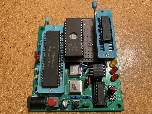
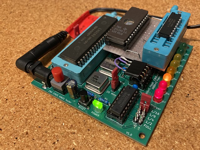
Meanwhile, I recently built up a Z80 CPU test PCB which was not my own design but an open source project. I was given the blank PCB along with some of the components - actually I swapped them for a spare 2708 EPROM programmer PCB which is another open source project along with a few parts for that. Details for both of those projects can be found in the links at the bottom of page.
Anyway I completed the build of the CPU tester and it worked well as intended. It tests the operation of the Z80 CPU at various clock frequencies and can also identify original type NMOS CPUs or later CMOS types by testing their response to some extended commands which are handled differently by the two types. A row of 8 LEDs serves to identify the IC type as well as confirming the function of the 8 data lines with a simple LED chaser effect.
Here's the CPU tester completed in its original form. There is no RAM on board and the entire 64k Byte address range of the Z80 CPU is directed to a 27C512 or equivalent EPROM of which only 420 bytes of code are used for the CPU test program.
To me, that immediately signalled a potential for this little PCB to perform some other useful task in addition to testing the CPU in question. Why not add some RAM and test that as well?
As it happens, I had already substituted a 27C256 EPROM as I had no 27C512s on hand, cutting the track which carried the upper address line A15 to pin 1 of the EPROM and linking that pin of the 27C256 (Vpp) to +5V instead. I had also chosen to use various coloured LEDs to make the LED chaser more colourful, these could be helpful to indicate RAM test Pass or Fail conditions.
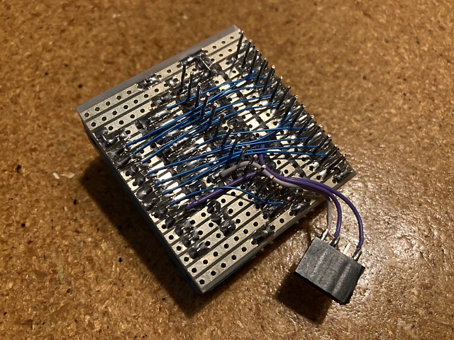
So, I made up a little board which plugs into the EPROM socket, most of the necessary signals are on there . I didn't have an 18 pin DIP ZIF socket handy so just used a 24 pin narrow ZIF socket which I had to hand, leaving the bottom 6 contacts unused.
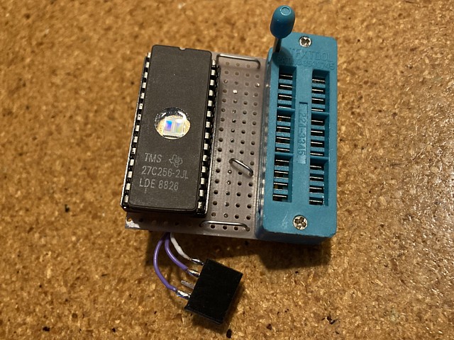
It's just a one off prototype built on a very small piece of Veroboard so all of the interconnections are done with wire on the track side.
- But could easily be built as a neat little add on PCB or added into the main PCB design without too much trouble...
I used a spare gate on the 74LS02 to invert A15, when high the EPROM is disabled and the RAM is selected. The other signal from the main board is the CPU /Write output.
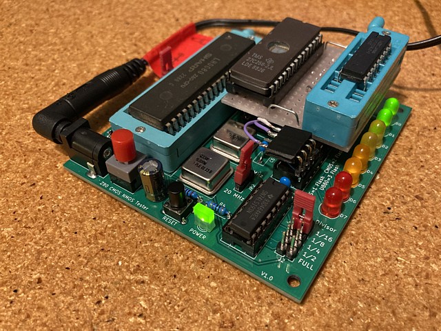
After the original CPU test completes one pass the RAM tests run. Lucky I used various colour LEDs originally. Two green = PASS.
Two red = FAIL and orange/ yellow indicate data or address range at fault. Above is a data error. The IC below passed the data test but was found to have a fault in one of its upper address lines A8 or A9. Yellow LEDs would indicate a fault in the lower address lines A0-A3 or A4-A7.
If no RAM is present the CPU test will still run and repeat as normal but will just indicate the RAM error in between passes. The extra code for the RAM tests is only a couple hundred bytes, taking the program size from 420 up to 656 bytes!
So the upshot with the previous RAM IC order for 10 pieces was 7 working, 3 bad. It is definitely a lot easier to test them individually, when installed into the computer it was pretty confusing to work out which ones were good and which were bad.
I'll add a little video to the links below and the extra code for the RAM test mod here:
Asm700.asm cpu_ram_test v1.0 Assembly listing
cpu_ram_test.bin v1.0 Hex file
This is just a follow on to the previous post about the 2114 RAM tester sub board, used in conjunction with the open source Z80 tester PCB. (scroll back for details and links)
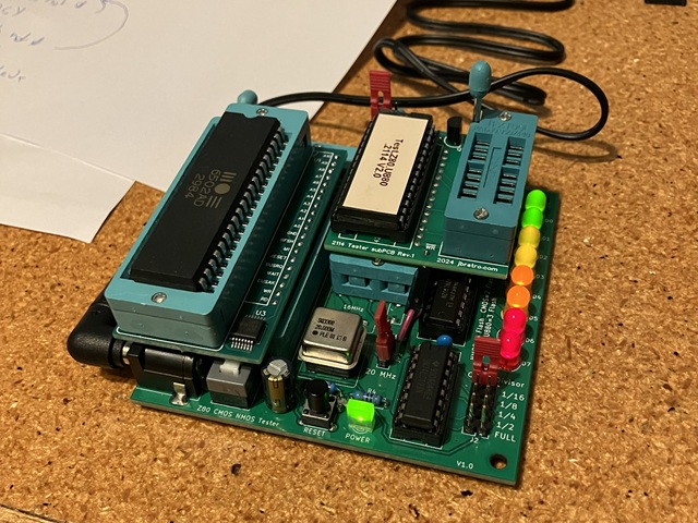
Going back about 12 months I made a single prototype on veroboard - which still works perfectly but taking on some good ideas by a friend we did end up with a PCB version and provision to swap the sub module for different types, to test other RAM ICs should that need arise.
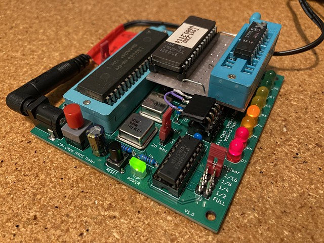
Here's the current version with the 2114 sub PCB. As per suggestions we've included a ZIF socket in the EPROM position of the main PCB so the sub board could be swapped if other versions are developed. That did mean the optional 16MHz oscillator was omitted but the main 20MHz oscillator is now socketed using a 8 pin DIL IC socket (with the centre 4 contacts removed) so either frequency can be easily substituted.
In practice the 20MHz version provides plenty of range with clock rates 1.25, 2.5, 5, 10 or 20MHz available by changing the jumper link. Using the 16MHz oscillator will produce 1MHz as well as intermediate rates 2, 4, 8 and 16MHz if required for testing CPUs at specific speeds.
The 2114 sub PCB now includes an 18 pin ZIF socket for the RAM under test and conventional 28 pin IC socket for the EPROM, either 27C256 or 27C512 types or equivalents can be used with a jumper link to select.
Address line A15 is still used to select either ROM or RAM, in the prototype I used a spare gate of the 74LS02 on the main PCB to invert A15 but to minimise interconnections between the PCBs I've added a transistor to invert A15 on the sub PCB. Apart from the 28 pin EPROM connector the only other interconnection required is the CPU /WRite signal so a single header pin is included with a wire link to the main PCB.
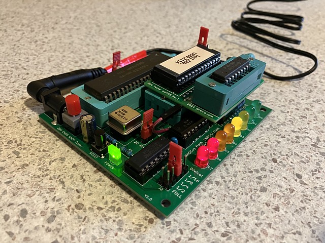
In the photo I'm using the module to test a couple of HM6148P-6 RAM ICs which I've just received from an OS order. They're an equivalent for the 2148H-3 used in Donkey kong, pin compatible with 2114 RAM but faster. Their markings look genuine but the pins have been re-tinned, these ICs have most likely been reclaimed from old boards.
Testing them with the 2114 module the first IC passed, the second result was a fail. The pattern of LEDs shown above indicates a problem with an address line in the A4 - A7 group. That is an unfortunate, 50% failure rate of ICs which were claimed to be 'brand new' but at least being able to test the ICs before fitting to a PCB under repair saves a lot of confusion and wasted time on the test bench.
Having produced the new 2114 subPCB I've since written an update for the 2114 tester firmware, adding a fastest possible fill of alternating 1010s and 0101s, with two passes to cover both possible patterns. To date the fast fill test hasn't managed to fail any RAMs which were otherwise passing the tests but it may catch out a slower than expected RAM at 10MHz clock speed, or higher depending on the CPU being used to run the test program.
The existing tests in version 1.0 could fail a very slow RAM anyway, in fact the fast fill routine doesn't change the write timing of the CPU so an individual write still takes the same time, just the time between consecutive writes is minimised and every write has all the bits flipped from the previous.
For the Z80 the fastest rate possible is by setting the stack pointer to the top of RAM then pushing the data to the stack - which is faster than the LDIR operation and doesn't require the pattern to be prewritten into ROMspace. It's actually just a 2 Byte (well, 2 nibbles really) word pushed to the stack 512 times in a loop.
Apart from that the tests run as before with led results:
D1, D0 = RAM PASS
D7, D6 and D5 = RAM FAIL (Data error)
D7, D6 and D4 = RAM FAIL (Address A8 - A9 error)
D7, D6 and D3 = RAM FAIL (Address A4 - A7 error)
D7, D6 and D2 = RAM FAIL (Address A0 - A3 error)
If all of those tests pass it moves on to the fast fill write and read back. If that fails there is a new error pattern:
D7, D6, D3 and D2 = RAM FAIL (fast fill readback error)
Here are links to the PCB, source and binary files if anyone is interested.
Gerber_2114_tester_PCB_v1_2024-08-09.zip PCB file
Asm702.asm cpu_ram_test v2.0 Assembly listing
cpu_ram_test_v2.bin v2.0 Hex file
Another update to the CPU / RAM tester project, having fitted a ZIF socket to the EPROM position on the CPU tester PCB and made up a 2114 tester sub PCB which can be easily removed or swapped for another type I've now also drawn up a version to test the 6116, 2k x 8 bit static RAM or equivalent such as 5116 etc. It's basically the same as for the 2114 except the memory range is 2k Bytes instead of 1k and the data 8 bits so there is no need for the software to mask out the 4 unused bits.
Although some EPROM programmers such as the common TL866 model can already test the 6116 RAM or equivalents those tests apparently don't run at high speed or allow the test routines to be altered. While fine for go / no-go tests it seems worthwhile to try an open source solution which can run various tests at multiple CPU clock rates and possibly identify an IC which has a slower than expected access time / speed rating.
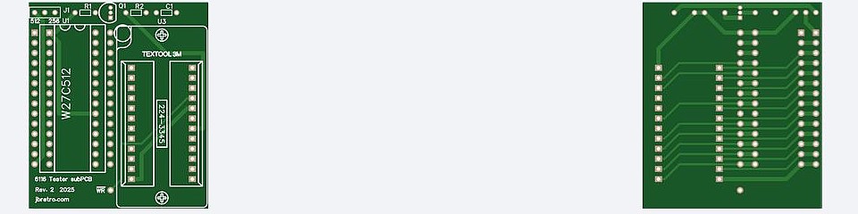
The PCB file is here Gerber_6116_tester_PCB_v2_2025-03-04.zip
and the program z80_6116_test_v2.bin
+source asm701.asm
I haven't been terribly organised with a Bill of Materials for the board so I'll just list the components here:-
1 x 28 pin IC socket for the (E)EPROM, goes to the left most set of pins e.g. Jaycar PI6507.
2 x 14 way header strips, standard length is OK e.g. Jaycar HM3212 but use long or round ones if you prefer.
- those go in the set of holes just to the right of the EEPROM, put them in first and make them flush with the surface on the parts side. Solder them in from the top...
1 x 3way header / jumper or just a bit of wire for selecting 27256 or 27512 EPROM size. ( Or Jaycar SS0834).
1 x 1way right angle header for the /WR signal. put above or below depending on clearance. (Or just bend one spare header pin).
2 x 10k resistor, 1/4W metal film types are a good fit for the PCB footprint.
1 x BC547 or equiv. - It's just a simple open collector transistor inverter to enable the RAM when A15 is high, easier than adding a 74LS04.
1 x 0.1uF ceramic / monolithic cap. (104) - The 0.1 uF is just across +5V and ground.
1 x 24 way 0.3 - 0.6" ZIF socket - Some equivalent RAM ICs come in the 0.3" narrow DIP format so a 24 pin ZIF socket which can accommodate either narrow or wide DIP packages should be used.
The test program operates as follows, it begins with one pass of the CPU test: should do 1 or 2 flashes of all LEDs then back and forth once with the LED chaser effect. Then it does the RAM tests. It tests for data errors then 2 passes to check for address errors and the last test is the fast fill data test. There are no LEDs during the RAM testing and the tests will be cut short as soon as any errors are found so the duration may vary if there are any errors.
Each pass of the RAM test takes longer to run than the 2114 version as the data range is 0-255 instead of 0-15 and the address range 0-2k. The address testing can do 8 bits at a time so there are only 2 passes required for that, address high or low byte compared to 3 passes for the 2114 version so the complete test if everything passes takes about 6 seconds at 10 MHz or around 45 - 50 seconds at 1.25 MHz.
If the test completes with no errors LEDs 0 and 1 will illuminate briefly then the CPU test will restart. If there are any errors, LEDs 7 and 6 will light up along with: 5 for data error, 4 for address error (high address byte), 3 for address error (low byte) or 2 and 3 together indicate all tests were OK except for the high speed test which failed. The program should loop continuously so you can see the error code each time after the LED chaser.
Also, if any of the LEDs don't light up during the LED chaser then the RAM possibly has a shorted data output. So the idea is to watch the LED chaser then look out for a pass or fail indication. I have some HM6116P-3 and LP-3 among my spares so tested those and all 3 passed every test at up to 10MHz CPU clock rate including the fast load and read back test.
To assist with a number of previous repairs I wrote some 'homebrew' test programs to run on various game PCBs, checking the RAM in circuit from the CPU's point of view. I've since ported the original programs to run on other game PCBs which employ similar hardware and think the program which I originally wrote to test some Exerion PCBs could be adapted to work on the Donkey Kong PCB set.
Both are Z80 based with separate RAM banks for background video / text and sprites as well as program RAM so with minor changes to the memory locations the program should run on the Donkey Kong Hardware. The video RAM is checked first which causes the jumble of characters on screen then once cleared the test results are placed into screen memory. For Exerion the text characters are Ascii based but the characters for Donkey Kong use different encoding so I've nicknamed it Donscii.
Unlike Ascii, codes 00 to 09 represent numeral characters 0 to 9, a blank space is represented by decimal 16 (10 hex) and upper case letters A to Z begin at code 11 hex. I haven't checked the remaining codes as other characters are not required for the test display, many seem to be segments of the background 'scenery' in the game screens. After assembling the adapted program and debugging in MAME it's ready to run on the actual Donkey Kong PCB set.
I don't have any spare 2532 EPROMs to load the test program onto so, comparing the pinout of the 2532 to the 2716 EPROM I realise as the test program is less than 2k Bytes a 2716 will work in place of the original 4k Byte 2532. The 2716 has 2 select inputs, /CE on pin 18 and /OE on pin 20 whereas the 2532 is selected when the PD/PGM pin 20 is low. Pin 18 on the 2532 is address input A11 which will also be low for the first 2k Bytes so the 2716 will work without any modification required.
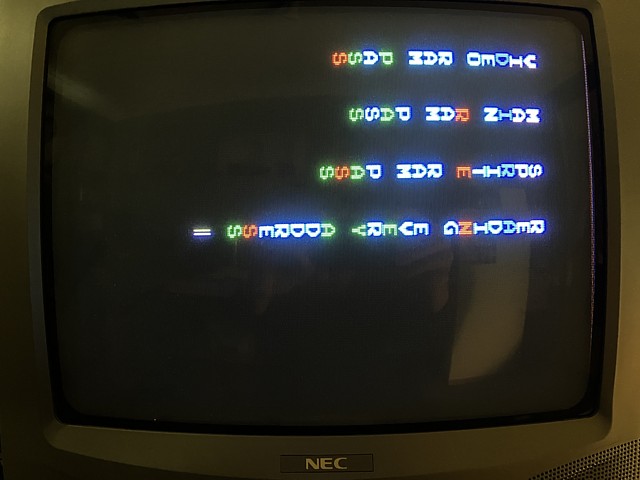
And with the test program loaded onto a 2716 EPROM then placed into the boot ROM position 5F of a TKG3, 4 board Donkey Kong PCB set - powering on the tests run and in this case each result is a pass.
Having successfully tested the RAM on a Donkey Kong TKG3 board set the test program should run equally well on the later TKG4, 2 board PCB set however I will make one small revision to the order of the test routines. The previous version would complete a single pass of each RAM area then proceed to an endless 'reading every address' loop, intended to assist with signal tracing within the PCB.
The latest version aims to identify marginal or intermittent RAM errors by completing a single pass of each RAM area followed by one pass of reading every address before looping back to the very beginning. At any point if a RAM error is found the program will halt with a fail message for the relevant section otherwise the tests will repeat indefinitely.
Placing the revised test ROM into the boot position of the TKG4 PCB set, powering on and allowing the test to complete several loops the results are as below.
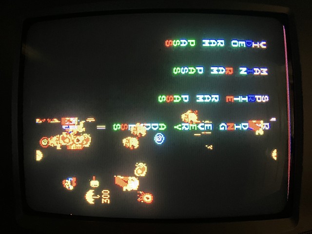
After several passes of the test routines the main, video and sprite RAM were all found to be working. Although the test program ran correctly and results are readable there is an unexpected, random looking pattern of sprites visible on screen. This may not be a fault and appears to be due to the contents of RAM on startup which have not been cleared. When I ran the same test program on the earlier, TKG3 PCB set however the sprite layer was not visible upon startup.
It would seem the sprite 'garbage' must be originating from the ECL RAM in the clock section of the video PCB as it remained on screen while the other RAM areas were all completely overwritten during testing. At this stage I don't think the symptom is a PCB fault or an error in the test program and doesn't affect the game program which must clear or hide the sprite layer upon startup.
So the RAM tests have completed successfully but in future revisions I may look to clear the sprite garbage from screen so the results can be displayed more clearly. One area which is not currently tested is the ECL RAM as this does not appear on the CPU memory map so is not directly accessible by the program to write data and then read back.
It should be possible to send a recognisable pattern of sprite characters to the screen via the ECL RAM as the hardware is configured to perform this task, although the results could not be read back by the CPU this would at least provide a visual indication if this section of the circuit is working correctly. That might be another task for a future revision, meanwhile the current version of the test software can be found here:
A while back I assembled a little test PCB for the Z80 Microprocessor which was an open source project (scroll back for details) and then came up with an extension which could also test 2114 RAM memory ICs using the Z80 processor with some additional programming of the on board EPROM. That has been incredibly useful, both for its original purpose of testing Z80 CPUs as well as any 2114 or equivalent RAM ICs which are found on many '80s era arcade PCBs.
My latest PCB repair involves a 6502 CPU rather than Z80 so I thought it would be helpful to have a similar tester which could verify the functionality of the 6502 at various clock rates as well as identifying either an original NMOS or later CMOS version of the IC. A quick search for open source designs revealed a few simple NOP style testers which repeatedly issue a 'No OPeration' instruction causing the CPU to advance through its address range but that was not quite what I had in mind.
Then I had a slightly different idea; why not make another extension for the Z80 tester which would adapt the circuit to use a 6502 CPU in place of the Z80 and perform a similar set of tests using the 6502 instruction set? That sort of idea just won't go away - I've never seen a circuit adapted to run with a completely different CPU, it seems a bit like doing an engine swap in a car.
And here's the result, using a simple adapter module and some additional programming the Z80 tester now has the ability to operate with the 6502. So how does it work, is it just smoke and mirrors? Well, no smoke thankfully but there is some mirroring involved due to the differences between the memory map of the Z80 and 6502 CPUs. Before going too much further it may be helpful to take a brief look at the similarities and differences between those two microprocessors.
Between them, the Z80 and 6502 CPU (and some of their derivatives) powered the majority of computers, consoles and arcade machines of the 8 bit era in the early to mid 1980s. Although very different functionally it is interesting that both began as non authorised, improved versions of earlier processors by established manufacturers; the Zilog Z80 building upon Intel's 8080 while the MOS 6502 spawned from Motorola's 6800 platform.
Not surprisingly, legal action prevented MOS Technology from producing the 6501, a pin compatible replacement for the 6800 but their 6502 made it to market with only slight differences. Both the Z80 and 6502 incorporated major features of their earlier counterparts along with new abilities. The 8080 instruction set effectively became a subset of the Z80's meaning programs written for the 8080 could run on Z80 based hardware, as happened in the case of several slightly later 'Space Invaders' clones.
In the mid 1970's Steve Wozniak's landmark Apple I computer board included options to work with either Motorola's 6800 CPU or the MOS 6502 with minor adjustments to the clock circuitry, as the less expensive 6502 became available during its development. Between the Z80 and 6502 CPUs there are similarities; both have 16 bit address and 8 bit data busses however there are many significant differences.
Of the two, the Z80 has more hardware inclusions with three 16 bit register pairs as well as the 8 bit accumulator, these can also be used as up to six 8 bit registers for storage of program variables without the need for external memory access. It also has separate external controls for memory or I/O access and the ability to free its address and data busses for direct access to memory by external devices (DMA).
The 6502 is considered by many to be a very powerful processor but in my opinion is notable for the hardware which was left out to reduce cost and complexity. On the other hand its instruction set includes address modes for fast access to external memory, alleviating the dependance upon internal registers. Although clocked at lower rates than the Z80, memory access occurs during the second half or phase of the input clock cycle reducing the number of cycles required for most operations.
Which brings us to the memory map. At power on reset the Z80 will read its first instruction, from memory address 0000 so the program ROM will be present from this address. In many cases the ROM will be organised into a continuous address range from 0000 to whatever with any RAM accessed at higher addresses. Even if several banks of ROM and RAM are used the very lowest addresses usually contain program memory (ROM) with any random access memory (RAM) beginning at some higher address.
For the 6502 the reverse is true. Although that CPU only has two internal 8 bit registers X and Y plus the accumulator A it has a 'Zero Page' addressing mode where access to the first 'page' of memory from 0000 to 00FF Hex is much faster as the 'page' byte 00 is not needed. This not only shortens the instruction saving program memory but makes the reading and execution of the instruction much faster.
Incidentally, Zero Page addressing modes did not originate with the 6502 processor or the 6800 for that matter and were already implemented in some of the earlier mainframe computers such as the PDP-8 made by Digital Equipment Corporation from the mid 1960s. It was a proven method of maximising performance from a time when computers had very limited resources.
So the first 256 bytes of memory are very useful for storage of program variables etc. as an alternative to internal CPU registers. The second page from 0100 to 01FF Hex is used for the memory Stack by the 6502 as its Stack Pointer SP has only 8 bits and always applies to the 256 Byte range within that page. This means the lowest addresses should always be reserved for RAM with program ROM located at some higher address.
At power on reset the 6502 will read a 'reset vector' from addresses FFFC and FFFD Hex, near the very top of its 16 bit address range. These locations must contain as data the 16 bit absolute address where the first program instruction is located. The 6502's program counter will then 'jump' to that address to read its first program instruction. As a result of this CPU architecture most 6502 based systems will position RAM at the lowest addresses with ROM in the uppermost address range.
OK, so how do we reconfigure the Z80 tester to work with the 6502 CPU? As it happens the Z80 tester in its original configuration has no RAM memory at all, its entire 16 bit (64 kByte) address range is allocated to the 27512 EPROM so there would be no problem adding the reset vector and locating the 6502 test program anywhere within the free EPROM space.
When I added the extension for RAM testing however I did need to allocate a section of the address range to RAM; the simplest solution was to use address line A15 to select either EPROM or RAM, effectively dividing the 64k Byte address range in half. So, even though the RAM under test was only 1k x 4 bits any address in the upper 32k Bytes would select the RAM while the lower 32k would remain active for the program EPROM.
Reducing the useable EPROM space from 64k to 32 kBytes might sound like a severe limitation but the entire 'Kinzi' test program included with the open source project was only 420 bytes long. Even with my added RAM testing routines the total program used less than 1k Byte of the total EPROM capacity. So to reconfigure the address ranges reserved for ROM and RAM we could invert address line A15 which would effectively swap the upper and lower 32k Byte address ranges.
That should work from an addressing point of view but the 6502 can't drive multiple devices attached to its address and data busses unless external buffers are added so I won't be using the RAM in conjunction with the 6502 at all. Instead of inverting address A15 I will just leave it not connected at the 6502 socket but linked to ground at the Z80 end of the adapter so the total address range becomes 0000 to 7FFF or 32k Bytes.
The only time A15 will be high at the CPU is upon reset when the reset vector at address FFFC and FFFD must be read however as A15 will be tied low at the EPROM end the actual addresses read will be 7FFC and 7FFD. Effectively the 32k Byte address range from 0000 to 7FFF wil be mirrored to also appear in the range from 8000 to FFFF Hex. The RAM socket which would be selected in this upper address range when connected to the Z80 CPU will not be active when the 6502 adapter is present.
Having no RAM does place severe limitations on the scope for programming the 6502 with no writeable zero page or stack memory the only storage for program variables would be the two, 8 bit X and Y registers and the accumulator itself. Also no subroutines can be called without any available RAM in the stack area to record the return address from the subroutine. A simple test program which is functionally similar to the original Z80 version should be possible.
So apart from rerouting the signals from the Z80 socket to 6502 pinout and leaving A15 tied to ground at the Z80 end the only active component required for the 6502 adapter is a 74LS00 NAND gate to convert the 6502's R/W signal to separate /RD and /WR in conjunction with clock phase 2 being active, as per this diagram from the '6502 User's Manual' by Joseph J. Carr. I'm using a surface mount, SSOP version of the 74LS00 to fit in the available space on the adapter PCB.
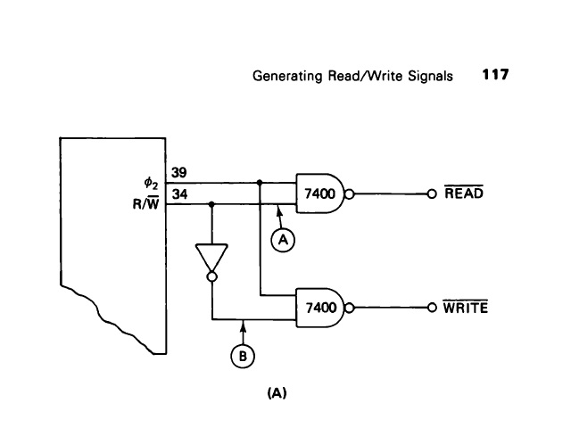
The /RD signal will enable the EPROM while the /WR signal will be active when writing to the bank of LEDs. In the Z80 tester circuit these signals are used in conjunction with /MREQ and /IORQ control outputs from the Z80 CPU, /MREQ becomes active when reading from or writing to memory while /IORQ accompanies an OUT() or IN() instruction i.e. to or from an I/O device.
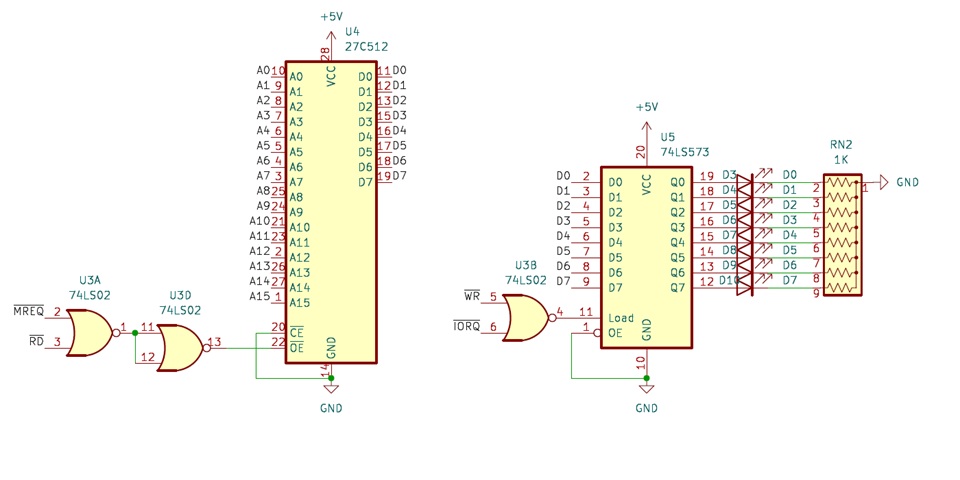
The 6502 however doesn't have a separate set of commands for I/O devices instead using memory mapped I/O. It simply writes or reads to or from an address so each input or output device should be selected by the address decoding circuitry. In this case there is only one device to read from (EPROM) and a single output device (LEDs) so specific address decoding is not required.
I'll simply tie /MREQ to ground so any read operation will enable the EPROM. Just to make some use of the otherwise not connected 6502 address line A15 I will route that to /IORQ so a write to any adddress where A15 is low (i.e. 0000 to 7FFF) will select the latch for the bank of LEDs. That will also make it possible to test the CPUs A15 output for correct operation as a write to any address where A15 is high (i.e. 8000 to FFFF Hex.) should have no effect.
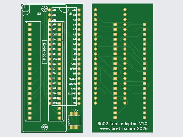
Here's a photo of the PCB layout. U3 is the 74LS00, U1 is the footprint for the Z80 connection. In this case header pins are added on the solder side which will plug into the 40 pin ZIF socket on the Z80 tester PCB. 2 Rows of 20 way round header pins can be used and should be placed so they are flush with the component side of the PCB then soldered from the top. Lastly, U2 is the additional ZIF socket for the 6502 IC to be tested.
And here is a listing of the 6502 test program which I have written thus far. I have assigned the starting address for the program as 4000 Hex which leaves the lowest 16k Bytes from 0000 to 3FFF Hex for the Z80 test software with the next 16k Byte block for the 6502 software from 4000 to 7FFF Hex. As the Z80 reads from address zero while the 6502 begins with the reset vector at the upper end of its address range both programs can coexist on the same EPROM.
6502 tester v1.0 Assembly listing
The 6502 test program operates in a similar fashion to the original Z80 test software. There is a single flash of all LEDs if the CPU is an original NMOS device, followed by a second flash if the CPU is a later CMOS type. Then a single pass of a LED chaser effect and the cycle repeats from the beginning. The test for NMOS or CMOS 6502 utilises a known bug in the original IC type which was corrected in the later, CMOS versions and relates to the JMP indirect instruction.
The indirect mode for the JMP instruction reads the absolute address of the jump destination (i.e. jump vector) from two consecutive bytes of memory however if the two bytes span across a page boundary e.g an indirect JMP command with an operand of 7EFF, instead of reading the second byte of the absolute address from the next consecutive byte at 7F00 it would instead read from 7E00.
So by placing a different 'page' vector in those alternate addresses we can jump to a different location depending whether the IC under test is a NMOS or CMOS variant. This has already helped me to identify a CMOS 6502 which has been re marked with the type number of an original NMOS device. Apart from testing for NMOS or CMOS versions the tester can verify the 6502 operation at various clock frequencies by selecting a crystal oscillator module and frequency divider setting.
The position for the crystal oscillator module is socketed so by using either a 12MHz, 16MHz or 20MHz oscillator with frequency divider setting from 1/16 to full, frequencies of 0.75MHz, 1, 1.25, 1.5, 2, 2.5, 3, 4, 5, 6, 8, 10, 12, 16 or 20MHz can be achieved. For the 6502 this should help to identify whether the CPU is an original spec. 1MHz IC, a 6502A capable of running at 2MHz, 3MHz 6502B or higher speed later model variant.
And with my pile of 'unknown' 6502 CPUs now identified and tested I can return to PCB repairs, once my latest order for some obsolete TTL ICs arrives from O/S. - More updates and test programs to follow in due course.
Web Resources (External Links) -
Z80 CPU tester modified to also test 2114 RAM ICs - YouTube
Z80 CPU tester PCB: djtersteegc/z80-cmos-nmos-tester - GitHub
Fluke 9010A Micro-System Troubleshooter - Centre for Computing History
All images and text on this website are Copyright.
Contact: jbtech at telstra dot com