Meteor (Asteroids clone) PCB repair
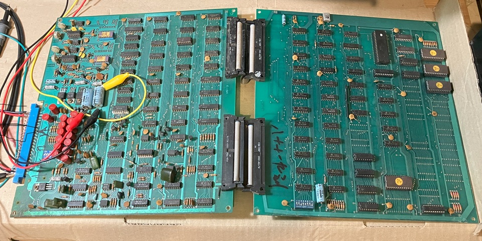
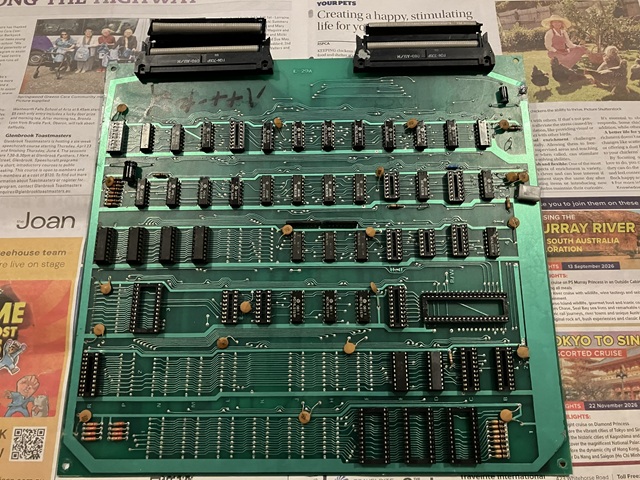
Here I have another PCB set on the bench for testing and repair. It's reportedly a Meteor, Asteroids clone by Hoei Intl. and appears to be a close copy of the Atari original. Although the layout appears very similar there is one notable difference; the Meteor circuit is divided into two halves connected by a pair of ribbon cables whereas Asteroids employs a larger single PCB.
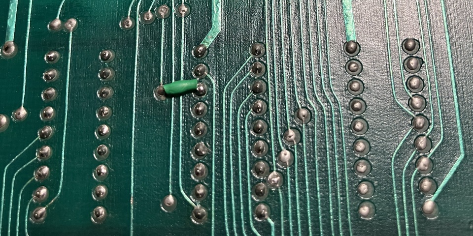
The Meteor PCBs aren't in great condition with some corroded IC legs and messy traces of previous repairs. Checking for any damaged or broken components I have noticed one issue - there is a row of inductors with plastic housings near the edge connector and the outer ones have been pushed over breaking their connecting leads.
I haven't found any circuit diagrams specifically for Meteor as yet so I'll refer to the very comprehensive Asteroids documentation and note any differences encountered. In the circuit extract below the 13 x 100 uH (microHenry) inductors are shown in line with the input signals with capacitors to ground forming a low pass filter arrangement. There is another pair of inductors nearby on the PCB, in series with the X and Y vector outputs.
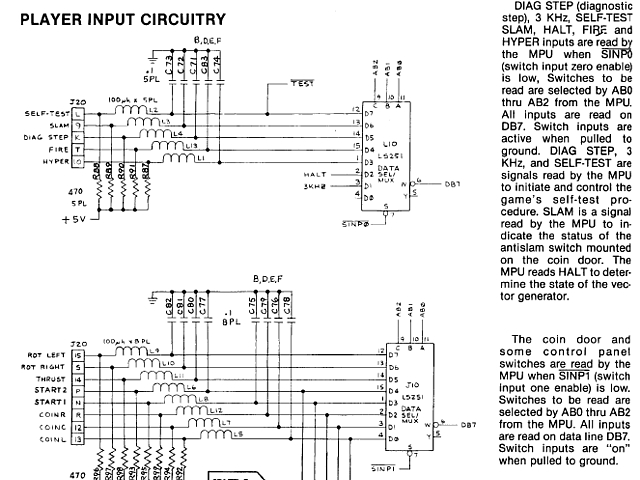
I'm not sure whether the input and output filtering was primarily intended to reduce glitching and switch bouncing of the controls, or to suppress any RF interference generated by the circuit to meet FCC standards - normally an L/C low pass filter arrangement would have the capacitors to ground on the load side following the series inductance - suggesting it is to filter incoming control signals but it may have been effective in both regards.
Although the inductors specified for Asteroids were 100 uH the ones fitted to meteor are marked 102 which would correspond to 1000 uH (or 1 mH) as I have confirmed by measuring one out of circuit with my multimeter. Fortunately the ones with the broken leads have just enough of a stub remaining to solder into the PCB so I have swapped these two to the X and Y output positions for the moment. I'll try and source some new replacements with my next parts order.
So the next step is to begin making up a test lead, set up power supplies and check for circuit activity.
I'm setting up a Meteor arcade PCB set for testing on the bench, beginning with connections for power only. I'm not connecting a monitor as yet, in fact I don't have a vector monitor to work with this game so will just use a Cathode Ray Oscilloscope set to X-Y mode and the Z input (which is available on the rear panel of the CRO) will control the beam intensity / blanking of the vector signals.
There is a 2 x 22 way edge connector for power and signal connections which appears to be pin compatible with Asteroids, I'll trace and confirm each connection with my multimeter just to be certain. Initially I'm just wiring up the +5V logic supply using a basic arcade switchmode PSU, the only other power connection required is 36 Volts AC (centre tapped) which is then rectified and regulated on board to provide the remaining DC Voltages required by the circuit.
I also don't have a transformer with a 36V secondary handy so will substitute an equivalent DC Voltage to the point on the PCB after the rectifier stage. But first I'll test the 4 diodes of the bridge rectifier with my multimeter to confirm none are shorted or open circuit and the correct forward Voltage shows on my meter display for each diode. Having done that I'll connect my bench power supply to the inputs of the on-board regulators at the smoothing capacitors C87 and C86.
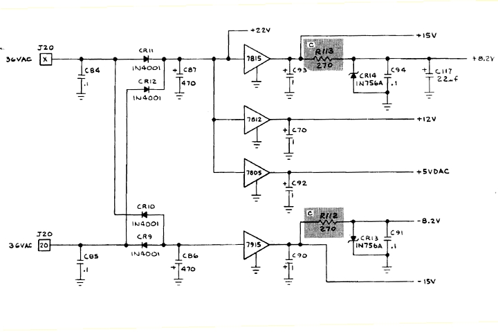
My bench power supply can manage plus and minus 20V DC at up to 3 Amps which should give enough headroom for the +/- 15V regulators to work correctly. I notice the circuit diagram indicates a nominal +22V at C87 and one would assume a similar negative amount at C86, also allowing for the forward Voltage drop across diodes and some AC ripple.
With the Voltages set on the bench power supply (+/-20V) and arcade PSU (+5V), powering on briefly to measure the regulated supplies on board the -15, +12 and the separate +5V supply (for the digital to analog converters) are present and correct but the +15V is missing. Power off, testing for a short to ground across the +15V rail does not reveal any problem so I suspect the 7815 regulator IC is most likely at fault.
That's a locally available part so after sourcing a couple of spares and replacing the IC in question, powering on once again the +15V rail is restored - but the zener diode regulated +8.2V rail now reads just over 10V so that diode must be open circuit. I don't have that value on hand so will try to source one locally and replace that component before powering on again.
I'm just getting back to this Meteor arcade PCB repair as I have been juggling a few works in progress of late. So far I have identified a faulty 7815 regulator IC and 8.2V Zener diode in the on board power supply regulator stage. Having replaced both of those all of the internal power supply rails are now present and correct. The next step will be to check for activity on the X and Y vector outputs in the unlikely event that the rest of the PCB is working correctly.
No joy there, both vector outputs show no sign of life when viewed with my oscilloscope so I'll check for activity further back, beginning with the signals at the 6502 CPU. If a board seems 'dead' with no output activity the usual starting point for troubleshooting is to check the CPU power, clock and reset lines followed by address, data and then control signals to see whether the CPU is active or idle, perhaps in a wait state or some sort of reset loop.
In this case there does seem to be some activity but the CPU reset input pin 40 is toggling so the CPU is repeatedly being reset, presumably by the watchdog timer. Many arcade PCBs especially those based on Atari designs include a watchdog timer to reset the CPU if the intended program flow is interrupted for whatever reason e.g. a power glitch, software bug or hardware issue.
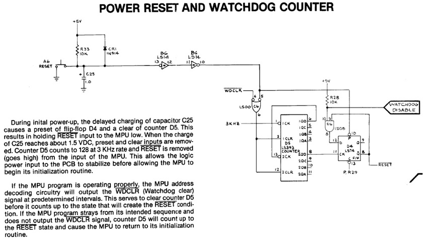
If the cause of the issue was a one-off glitch then normal operation will automatically resume after reset but a more serious fault will cause the watchdog timer to reset the circuit repeatedly, as is happening in this instance. The Watchdog timer is exactly that, a counter which will cause a CPU reset after a certain delay. In normal operation the timer must be accessed by the CPU program at regular intervals to restart its count. If that does not occur the timer will reach its limit and trigger a CPU reset.
Interestingly the reset signal in this case is not repeating at a steady, regular pace but with varying intervals which suggests the program is operating to some extent and clearing the watchdog timer initially but stalls at some point allowing the watchdog timer to reset the CPU and the cycle then repeats. The most likely cause of a CPU which begins to run but ends up in a short reset loop would be a ROM or RAM fault so I'll try to verify those components out of circuit to begin with.
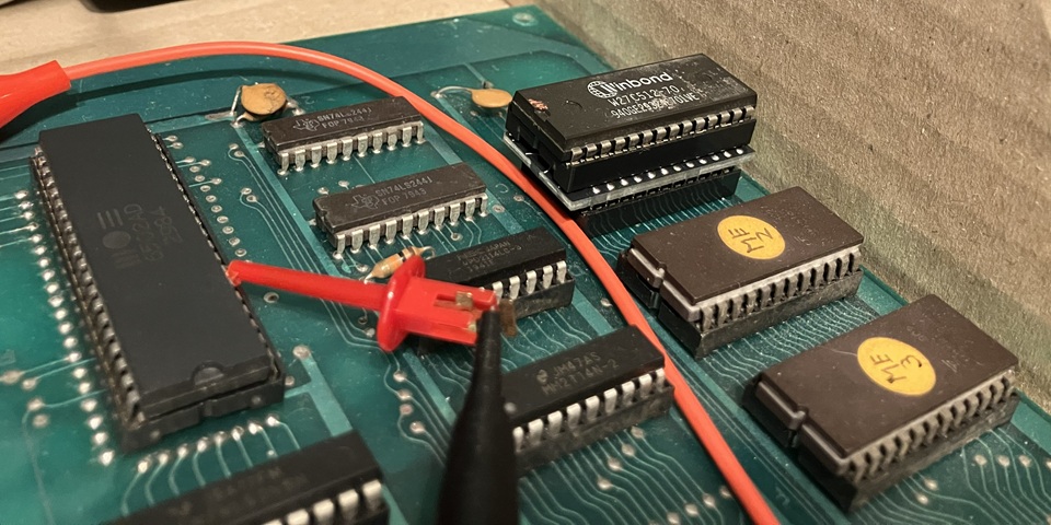
Fortunately both ROM and RAM are socketed on this PCB. The four MB8516 EPROMs are labelled ME1 to ME4, they're 2716 equivalents so can be read with my EPROM programmer and verified against known MAME ROM sets using an online ROMident utility. Having done that all 4 are exact matches to known ROM files, two are identical to Asteroids ROMs while the other two match up with an Asteroids clone called Aerolitos.
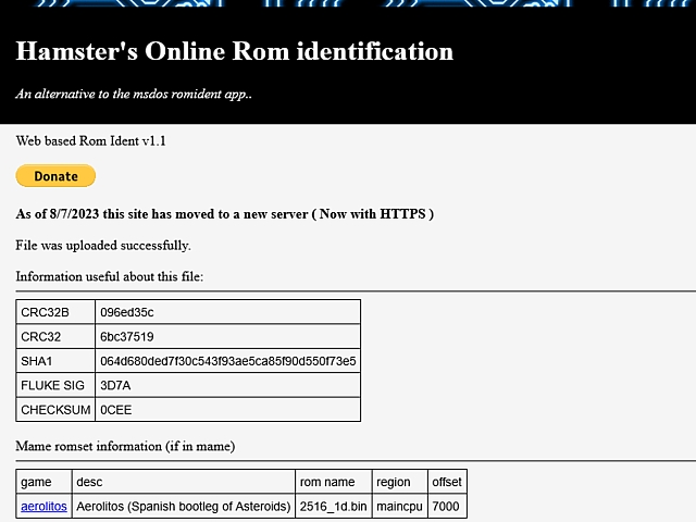
Incidentally, there is a known ROMset in MAME for Meteor by Hoei Intl. but that set is read from 8 x 1 k Byte ROMs whereas this PCB is fitted with 4 x 2k Byte EPROMs. The easiest way to directly compare this version to that known set would be to first divide each of the 2k Byte files in half. As there is a relevant match for the existing 2k Byte EPROMs there is no need to take that extra step, the EPROMs and their contents must be working correctly.
Next testing the 6 x 2114 static RAM ICs using my CPU / RAM tester, two of the vector RAM ICs fail the tests with data errors. Fortunately I still have a few spare 2114 ICs on hand so I'll place the 4 ICs which passed the RAM tests into the vector RAM positions and the two replacement ICs (which are also tested and working) into the CPU RAM positions on the PCB.
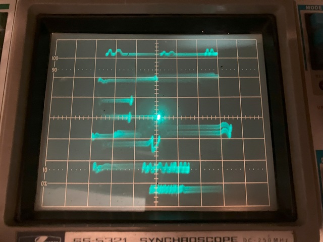
That done and powering on once again there is a definite improvement with the CPU reset line now remaining high after initial reset so the program seems to be running without crashing. Checking the vector outputs once again there is a repetitive short burst of signal on the X axis but just some noise on the Y vector output. At this stage there is no point viewing those signals in X-Y mode so I will trace back from the Y vector output to see if i can find a point where that signal goes missing.
Continuing with the fault tracing on the Hoei Meteor PCB set; to date I have checked and repaired the DC power supply regulator stages, replaced a couple of faulty 2114 RAM ICs and resoldered two inductors which had broken leads. When the circuit is powered on I am now seeing a repetitive, short burst of activity on the X vector output but only some low amplitude noise on the Y output.
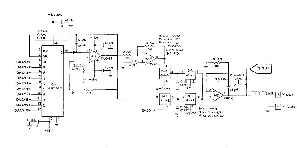
Referring to the (Asteroids) circuit diagram once again, the Meteor output stages appear very similar and the good news is there does appear to be some activity at the output of the Digital to Analog Converter. Following that is a CMOS analog switch, in this instance a 4066 IC is used rather than the 4016B shown in the circuit diagram.
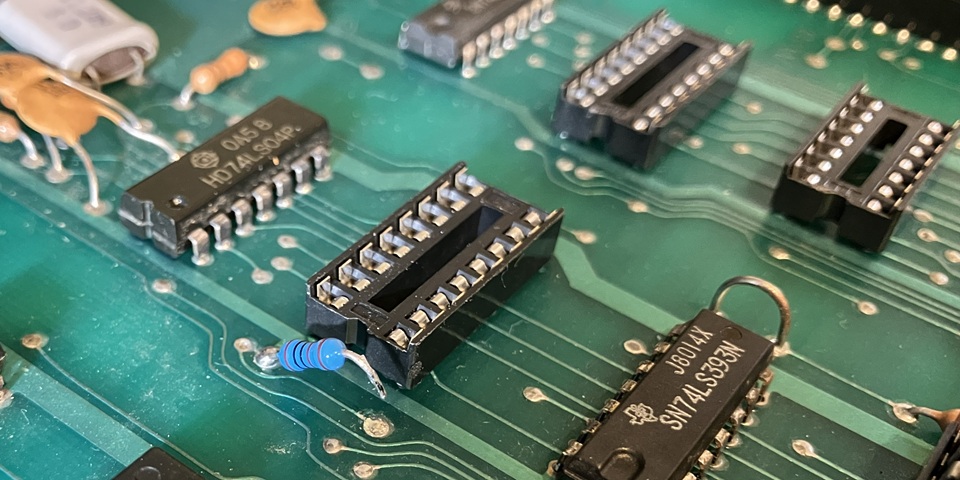
Checking its outputs there appears to be just some DC offset with no signal activity, it could be the IC itself which has failed or a poor connection due to severe corrosion of its pins. It's not just a bit of surface rust, the IC legs seem to be almost rusted through and the IC socket appears to be similarly affected. I have some 4066 ICs to hand so will replace this one as well as the IC socket.
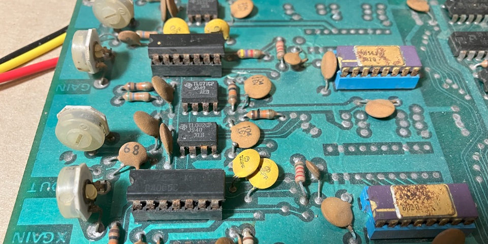
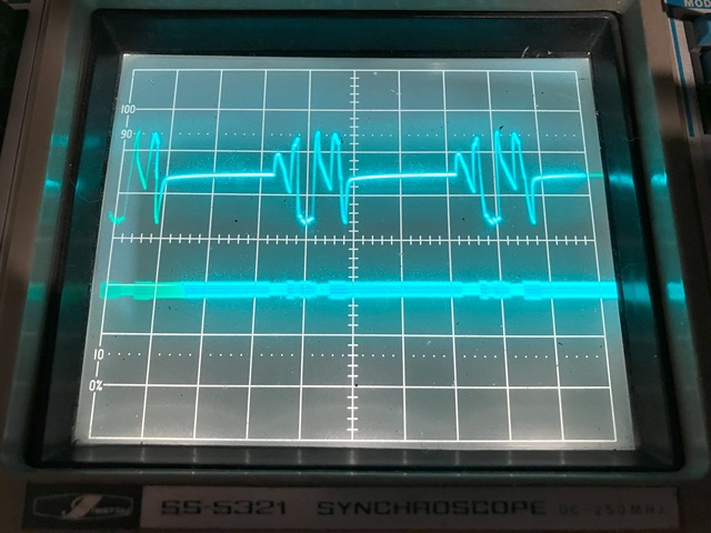
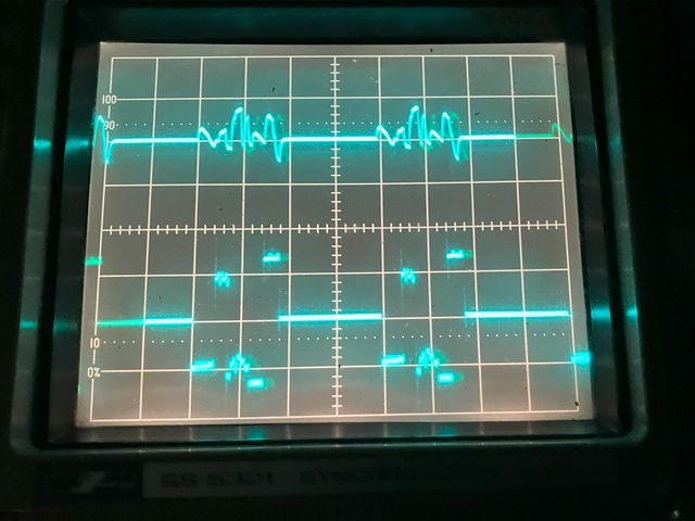
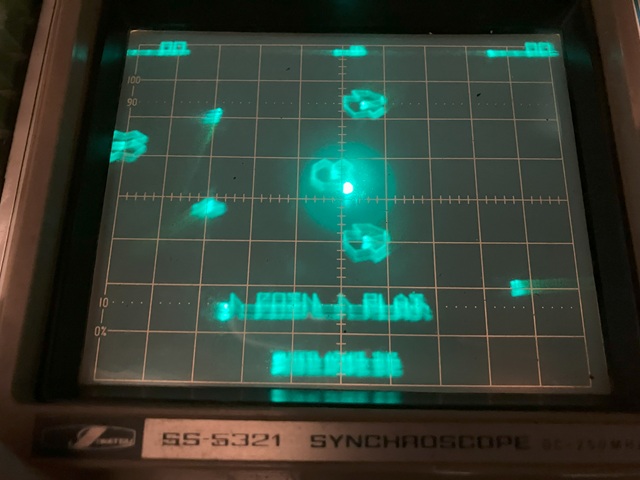
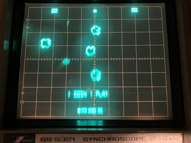
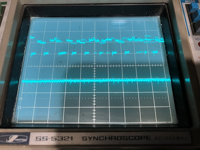
The corresponding IC on the X vector output stage doesn't look much better so I will also replace that one in due course but for the sake of fault tracing will leave well enough alone for now. So, after replacing the 4066 IC in position B12 along with its socket the X and Y vector outputs are now both showing little bursts of activity. Switching the Oscilloscope display to X-Y mode there is some sort of image:
As yet I haven't connected or even checked the Z (intensity) signal from the PCB so the entire path of the X / Y outputs are visible including a bright centre spot, not only where valid characters are present. To avoid phosphor burn I only turned the brightness up briefly and just enough to make the traces visible for the above photo.
The image seems pretty indistinct so there may still be some graphics issues but the program appears to be running, in attract mode with the Asteroids - er, Meteors drifting around and some text message on screen. Switching back to 2 channel display the Y vector output now looks sharp, by comparison the X vector output appears low in amplitude as well as having a poor slew rate.
That could be an op-amp problem but I'll begin by replacing that second rusty 4066 IC and socket to see whether it resolves the issue: That done, the image now looks much better with some recognisable shapes and text. The next step will be to check and connect the PCBs Z output signal in order to see the displayed characters more clearly.
I'm making slow progress with the Hoei Meteor PCB repair; the game runs now in attract mode and I can see the vector graphics on my oscilloscope display in X-Y mode albeit not clearly as yet. To see the vector lines which make up the image without all of the intermediate traces (as the beam jumps from the completion of each line to the start of the next) I need to connect the PCBs Z axis (intensity) signal to the Z input on the rear panel of my oscilloscope.
The Z signal determines not only the blanking but also the relative intensity of the vectors which are to be displayed. Reading the Atari Asteroids circuit description, the blanking level of the Z Output is 0 Volts with +1 to +4 Volts for the range of intensity determined by the 4 bit SCALE signals, giving a possible 16 shades of grey (or green as viewed on the oscilloscope display).
So the Z output is effectively a positive video signal, with higher Voltages resulting in a higher display intensity. Checking my oscilloscope manual however a positive going signal on its Z input decreases intensity, to obtain a correct image I will need to invert the Z Out signal from the Meteor PCB.
To achieve that I can use my video inverting amplifier which I originally built and used for testing a Nintendo Space Firebird PCB set. Since then I have used it for other Nintendo games from Space Fever to Donkey Kong as all of these titles originally used a Sanyo monitor which required a negative going video signal. The amplifier has 3 identical channels to invert an RGB signal
In this case I only need a single channel to invert the monochrome Z signal from the Meteor PCB and the input termination is not required but I will leave the 75 Ohm terminations switched on for the other two inputs so they are not left floating. Having done that the vector image on my oscilloscope display is much improved but still not perfect.
The main problem now appears to be an instability in the Y axis causing a blurry ghosting or double image vertically on the oscilloscope display. It's most noticeable on the text characters, I think this is a fault in the Y channel of the Meteor PCB rather than a problem with the test setup or general power supply issue which would most likely affect both X and Y axes equally. So I'll need to check for noise on the PCBs Y axis output.
The Meteor PCB is running now, on the test bench and displaying its attract mode using my oscilloscope display in X-Y configuration as a vector monitor. The Z (blanking / intensity) signal is also working with the addition of an inverting amplifier to adapt the signal to the format of the oscilloscope's Z input. So far the display looked sharp in the horizontal axis but blurred in the vertical, presumably due to noise on the Y axis output from the PCB.
Switching the oscilloscope back to conventional 2 channel mode to compare the background noise of the X and Y channels, both signals look clean up to the final inductor which is in series with each output. The Y signal after the inductor shows an increased noise level probably due to a poor connection, high resistance or dry solder joint from the output side of the inductor to the circuit board.
Looking back, I had found a couple of inductors with broken leads on the control inputs to the board and (temporarily) swapped those to the X and Y outputs, soldering the short stubs which remained of the broken leads into the PCB pads. At the time I also ordered some replacements which have since arrived so, removing the old inductors from both X and Y channel outputs and replacing with new components we now have a nice looking vector display.
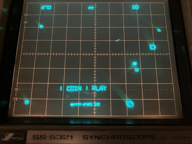
A quick test of the control inputs with a wire link to ground shows the game does appear to coin up and start with ship controls and firing also working. The next step will be to add connections to my test setup for joystick control and audio output, test the game functions and sounds to see whether all are working.
Although the Meteor PCB now runs there seem to be several issues yet to resolve. I have connected a joystick to the main control inputs; rotate left /right. thrust, fire and hyperspace which all work as expected however the PCB occasionally resets mid game or during its attract mode, presumably the program is crashing intermittently and the CPU is then reset by the watchdog timer.
I've also connected a small amplified speaker to the low level audio output from the PCB. The explosions can be clearly heard but the rest of the sounds are either completely missing or sound wrong. The firing sound is just a high pitched beep with no dynamic character and the thump sound which increases in tempo as the game progresses is barely audible as a faint click.
I'll return to those sound problems later as my priority is to resolve the program crashing issue which does seem to occur more frequently as the PCB warms up. It may be possible to localise the problem to a specific area on the PCB by selective heating and cooling and I should also look for any marginal signal levels around the CPU address and data busses.
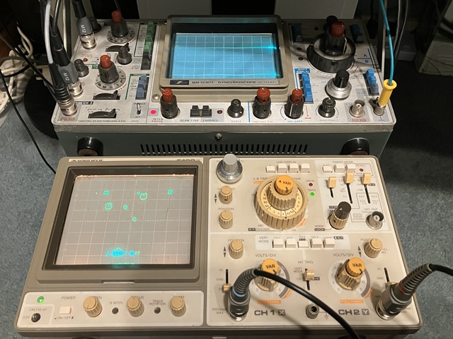
To probe around the signals within the circuit while still observing the vector display output I'll need to press a second oscilloscope into service, to function as my vector monitor and return my usual test bench CRO to signal tracing duty. My test setup for this PCB set is looking pretty busy with 2 separate power supplies as well as additional sound amplifier and vector display. For more common raster video games my usual test bench RGB video monitor would suffice.
As I prepare to observe the address and data signals around the CPU I have discovered that just touching that IC can sometimes cause the program to crash and reset continuously, pressing lightly at either end of the 40 pin package seems to return it to normal operation. That is obviously caused by a poor connection, most likely the old IC socket with single-wipe contacts is to blame. I don't routinely replace IC sockets for no reason but this one definitely needs to go.
Removing the CPU in order to replace its socket I've just noticed another problem; the IC is marked as a MOS MPS6502 with date code 1280 (presumably 12th week, 1980) but a higher speed 6502A should be fitted here. It was obviously working to some extent but could definitely be responsible for the random crashing and resetting problem so also needs to be replaced with a working 6502A. The Asteroids circuit diagram specifically notes this detail:
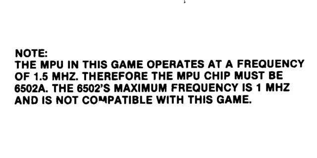
The CPU on this PCB was almost certainly replaced at some point, there is a dot of white paint on it where it has been marked by a previous repairer so we can only guess whether that was to signify if the IC was tested or maybe used as a temporary replacement during a repair. Another suspicious detail is the IC has another marking and contradictory date code - KOREA 3679 on its underside so the markings on top which suggest it is a genuine MOS branded 6502 are probably fake.
So, I have ordered a couple of replacement ICs; these ones were advertised as MOS 6502A CPUs and I chose a local online seller in the hope of obtaining genuine New Old Stock items. Although they were shipped locally and did arrive very quickly from order they unfortunately bear all of the telltale characteristics of fake, remarked ICs and were most likely sourced from disreputable suppliers overseas to be resold locally.
Both have different markings on their underside which appear to contradict the identical type number and date codes which have been printed on the top face of the ICs. The first is marked underneath as R6502F MEXICO 1327. Although it does run when installed on the PCB it exhibits the same random crashing behaviour of the previously fitted CPU and is most likely another 1MHz rated 6502 IC rather than the claimed 6502A specification.
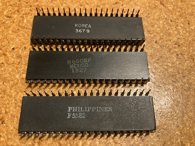
The second IC is marked PHILIPPINES F5582 on its underside and does seem to run correctly without crashing when installed on the PCB. Although advertised as a MOS 6502A I suspect this one could be a later CMOS type 65C02 or equivalent which at least seems capable of running reliably at 1.5MHz. As it appears to work correctly in this instance I will leave it installed as it seems almost impossible to find a genuine replacement part with correct markings.
Moving on to the next problem, I have noticed the vector image is not stable but tends to jump slightly in the horizontal, X axis. As the CPU crashing issue now seems to be resolved this must be an unrelated fault around the area of the X axis Digital to Analog converter or analog output circuitry.
I have been making slow progress with the Meteor PCB set which has been stranded on my test bench for a very long time due to other higher priority commitments. Now it's time to complete the repair and move on to new projects. In the last installment the PCB was running without crashing and exhibiting only minor image instability along with some sound issues. Cue the secondary fault!
The 'secondary fault' is a common theme within my repair logs which usually describe my attempts to revive long abandoned PCBs with no known history, probably years of disuse and storage in less than ideal conditions. Once any initial symptoms are addressed and the PCB is seen to be working to some extent a secondary fault often occurs which sets us back to a non working condition. In these cases we must restart the fault tracing from the beginning.
Powering on now there is a random looking vector display with lines darting about and no recognisable pattern. The watchdog timer is once again resetting the CPU continuously. There is a test point on the PCB to disable the watchdog timer; when grounded the random pattern continues with little change - the CPU seems to be running but has derailed from its normal program flow at some point.
Before commencing any new fault tracing I will take a step back and verify the components which I have previously tested are still working. RAM and EPROMs still test OK when removed from the PCB as well as socketed logic ICs. The fault symptoms are unchanged when the CPU is swapped and there is no apparent change once the ICs are reinserted in their sockets so the problem seems to be more than a simple socket issue.
Rechecking the power supply rails reveals no problem in that area so I will do some signal tracing to see if there is any obvious reason why the watchdog timer is not being reset. The /WDCLR signal should become active when the CPU performs a write operation to address 3400 Hex. The data written to that address is unimportant, it is the signal generated within the address decoder which causes the watchdog counter to be reset.
The Meteor / Asteroids clone PCB repair has taken a backward step; what was previously running with video and controls working is now failing to start and stuck in some sort of reset loop. A quick probe around clock, address, data and control signals reveals no glaring errors so the new fault will require some more detailed analysis to resolve.
On one hand an intriguing problem with no obvious cause can be an interesting and rewarding challenge to unravel. On the other, I don't have much free time at the moment to immerse myself into the finer details of the circuit design - this could take a while. To begin with, the watchdog timer is repeatedly resetting the CPU. Its counter appears to be working but the /WDCLR signal which should be created by the program at regular intervals is inactive.
That could be due to a fault in the address decoding circuitry which is responsible for the memory-mapped I/O ports as well as the program and graphics RAM and ROM assignments. It could also be caused by an address or data error derailing the program flow to the extent that it does not process the instructions to output a signal to that address.
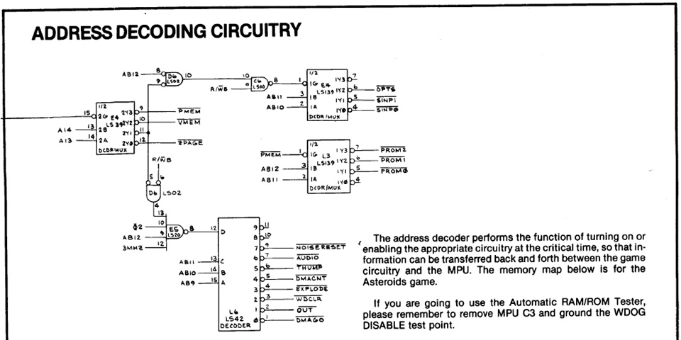
Before moving on to some actual checks and results I will attempt to summarise the workings of the address decoder circuit so feel free to skip this part if not wanting to know the theory behind the circuit design. And yes, I realise one can simply ask an AI chatbot to explain this circuit but bear in mind that AI works by regurgitating knowledge and content harvested from the internet - which has been shared by real people, some correct and sadly a great deal either flawed or misinterpreted.
Referring to the circuit excerpt above, the address is decoded in stages beginning with IC E4 at the top left of diagram. Its enable signal pin 15 is shown as either coming from CPU A15 or linked to ground, as the upper 32k address range is unused A15 is normally low (except at reset when the 6502CPU reads its reset vector address - more on that later). So this stage is always enabled and one of its outputs will be low depending on the address selected by the CPU.
Specifically address bits 13 and 14 determine the selection; when both low (address range 0000 to 1fff hex) the /ZPAGE signal is active low, selecting the program RAM. When A14 is low, A13 high (address 2000 to 3fff) the I/O addresses are enabled; if buffered address AB12 is low and buffered read/write R/WB signal high then inputs at address 2000 to 2fff can be read. AB12 high and R/WB low allows outputs within address range 3000 to 3fff to be written to.
A14 high, A13 low (address 4000 - 5fff) selects video memory. As both vector RAM and vector ROM are within this address range the address is further decoded within the video section of the circuit. Both A14 and A13 high (address 6000 - 7fff) selects the program ROM range which is further decoded by IC L3 into 2k Byte blocks /PROM2 (7800 - 7fff), /PROM1 (7000 - 77ff), /PROM0 (6800 - 6fff) and unused (6000 - 67ff). PROM2 is the 'boot' ROM, more on that to follow.
Getting back to the /WDCLR signal, that is further decoded by IC L6 from the output address range 3000 to 3fff. The 74LS42 is a BCD (binary coded decimal) 1 of 10 decoder but its D input pin 12 is being used here as an enable signal - when high the unused outputs 8 or 9 will be active, when low outputs 0 to 7 will be selected depending on the state of address lines A11, A10 and A9.
Each output of IC L6 then will correspond to a 512 Byte address range beginning at 3000 hex, 3200, 3400 etc. with output 2, pin 3 being /WDCLR. A write to any address from 3400 to 35ff hex would cause this output to be selected but for the purposes of programming it is defined as 3400 hex. In binary that is expressed as 0011 0100 0000 0000 i.e A15 low, A14 low, A13 high, A12 high, A11 low, A10 high and A9 low with address bits 8 to 0 determining the range from 3400 to 35ff Hex.
The Meteor PCB set has been on my test bench for eons and I seem to be light years away from getting it working once again. Its repair recently went off course from an almost working board with minor issues to 'Houston, we have a problem'. After re-testing memory components and checking signals around the CPU there are no obvious issues there so I'll look for clues in the area around the address decoder.
Referring back to the previous image which shows the address decoding circuitry, checking outputs of IC E4 reveals all address ranges; Program ROM, Vector RAM/ROM, I/O addresses and program RAM are active with the buffered CPU Read/Write signal also active. Checking the most obvious symptom, the lack of a /WDCLR signal from IC L6 reveals no activity on any of its out puts 0 -7 due to its D input pin 12 remaining high.
That comes from the 74LS20, 4 input NAND gate in position E5. A quick check reveals all of its inputs are active so it seems that could be faulty. For its output to be low all 4 inputs must be simultaneously high though that is not straightforward to confirm with a 3 channel oscilloscope - I guess I could view 3 of the inputs while using the 4th as an external trigger source for the B timebase but it seems easier to remove and socket that IC position, try a replacement which I have to hand.
Although that doesn't get the PCB running there does seem to be a change with some activity on the outputs of IC L6 but still no repetitive /WDCLR signal. At this stage I'm not sure if that represents an improvement or just a different pattern of signals each time the board is powered on. It could be L6 has problems and its input has been loading the output of E5 so as a last resort I'll try removing, socketing and replacing the 74LS42 in position L6.
That makes no improvement and seems to confirm that this part of the circuit is not at fault, rather the program is not writing to these I/O ports as intended. In these instances a logic analyser could be used to great effect but without that resource my next option is to substitute a small test program for the program ROM to create some predictable activity which can be traced using an oscilloscope.
I should mention that Asteroids does have an inbuilt test program which uses audio tones to confirm RAM operation and vector output with simple test pattern also displaying DIP switch settings, unfortunately that does not seem to run correctly with no display output or noticeable sounds. The PCB does have sound issues so the RAM tests may be running but without any audible indication. So substituting a simple test program into the 'boot' ROM position seems the next best option.
I've written a number of test programs for various arcade PCBs, the most recent and most elaborate ones have been for Z80 or 8080 CPU based boards with raster display. My earliest attempt was a simple program loop for the 6502 CPU in Missile command so it should be straightforward to adapt that one to run on the Meteor / Asteroids clone PCB.
The program loop was intended to simply read each address from 0000 to 7fff in sequence, also writing to specific I/O addresses at regular intervals to clear the watchdog timer and output pulses to the Player 1 and 2 Start LEDs to signal activity. If the program runs correctly that will confirm the CPU is able to read from the boot ROM as well as write and read the loop count from the Zero page of RAM.
Using an oscilloscope it should be possible to confirm all address selections within the address decoder circuit become active in sequence each time the program loops around. The boot ROM and RAM select lines should show constant activity as these addresses contain the program instructions and loop count data. The adapted program will need to be loaded into a 2716 EPROM and fitted to the 'boot' PROM2 position in place of the original program EPROM ME1.
So having done that and placing the ME1.x04 test EPROM into the boot ROM position, powering on - the program does not run correctly and the watchdog timer resets the CPU repeatedly. This was not completely unexpected and confirms there is some fundamental issue causing the program to be misread, most likely an address or data signal integrity issue. At least with a short, simple program it should be easier to determine the exact point where it all goes wrong.
Coming back to the Meteor PCB repair once again I'm trying to locate the cause of the latest fault which is preventing the program from running, using a short test program loop to create predictable activity on the CPU address and data busses etc. Even that program is crashing, suggesting a fundamental problem accessing or reading program instructions from EPROM or writing and reading data from RAM.
Using the oscilloscope to view the address and data signals at the program EPROM I'm concerned by the irregular amplitude of the address lines in particular with the high and low signals being quite uneven. It seems there is some sort of crosstalk between address lines causing steps in the waveform. Although most obvious on the high signal level that may not be causing errors as a valid TTL logic High can be anywhere from 2.4 - 5.25 Volts.
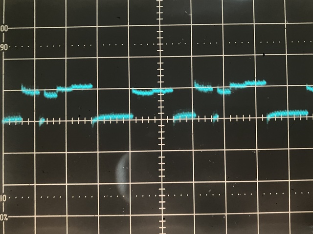
Of more concern is the curved, slightly rising low signal level, to be a valid TTL logic low the signal must be 0.8 Volts or less. Here there appears to be at least 0.5V of variation in the level, possibly more. At best I would consider this signal quality as marginal. This sort of signal interaction and rounded waveform could be caused by poor connections especially a missing or high resistance ground connection to the EPROMs or associated logic.
Checking the resistance from the ground pin of each IC to nearby ground tracks on the PCB I can't see any obviously missing or bad connections. The other area of concern would be the old single wipe IC sockets used for the EPROMs. Testing the bussed connections from each pin on one EPROM to the same pin on adjacent ICs gives very inconsistent results with some readings of a few Ohms so it seems these should be replaced with new dual wipe sockets sooner rather than later.
Taking the time to replace all four EPROM sockets has improved the continuity between IC pins and PCB tracks but sadly has not cured the current fault symptoms so I'll turn my attention to the address and data buffers. The 74LS245 data buffers were socketed and the ICs appear relatively new compared to other ICs on board. I have tested them out of circuit and they seemed fine but the sockets appear to be original style with single wipe contacts so I will also replace those for good measure.
The 2 x 74LS244 address buffers were not socketed and appeared to be as originally fitted to the PCB. Although each output was active the aforementioned level variations were also observed at this stage while the inputs from the CPU were regular looking square waveforms with correct levels. I have some spare 74LS244s on hand so will remove and replace these with new ICs and sockets. That done the result is unchanged but at least it's one more possible cause eliminated.
So with potential socket issues rectified and still no clear indication of the main problem I'd like to confirm whether the CPU is reading its program instructions from EPROM correctly before moving on to test RAM and other parts of circuit from the CPUs perspective. To do that I'll begin with an even simpler test program then add more test routines as each stage is confirmed.
The initial program will be the simplest test imaginable. Upon reset the 6502 will always read its reset vector which is the starting address for the program, From address FFFC and FFFD Hex. (as the uppermost address bit A15 is not used on this PCB the actual locations reached will be 7FFC and 7FFD) the data at these locations will point to address 7800 Hex, the starting address of our test EPROM.
The EPROM will be filled with NOP (No OPeration) instructions, assuming these are read correctly the program counter will just advance by one. The CPU will read its next instruction, and so on. At the end of available EPROM space a jump instruction will return the program counter to address 7800 Hex and the process will repeat. The CPU address lines should appear as square waves as the program counter advances from each instruction address to the next.
Although I would normally just burn the test program into a spare EPROM of the same capacity (in this case a 2716), I don't have many spares of this type. They are well obsolete and the last batch which I bought had a high failure rate so instead of repeatedly erasing and reprogramming one of my few spare 2716 EPROMs I will make a simple adapter for the relatively common W27C512 EEPROM, to work in place of the original 2716.
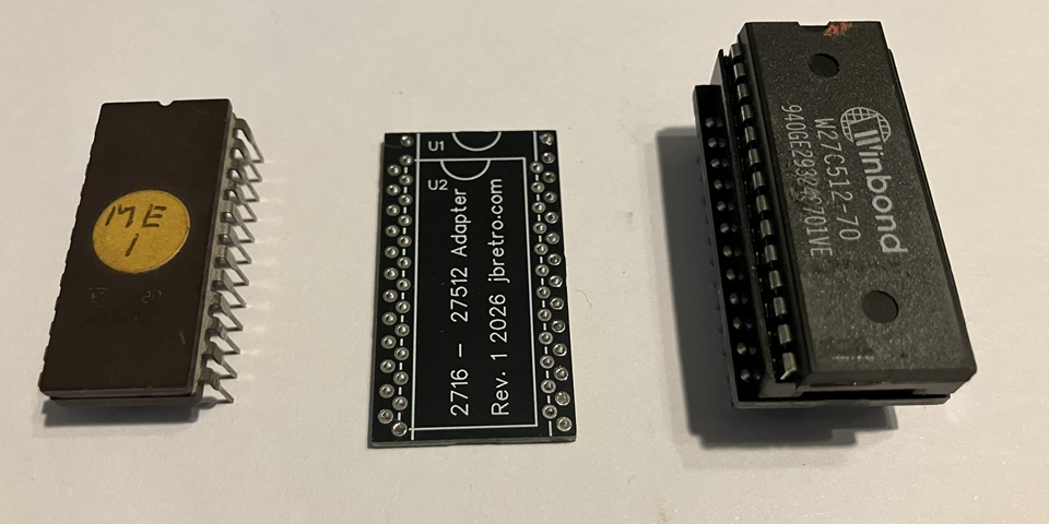
This will allow me to easily add revisions to the test program and write the latest version to the EEPROM. Being electrically erasable there is no need for Ultraviolet erasing and my TL866 EPROM programmer can erase and reprogram the IC within a few seconds. And placing my minimal test program with adapter into the boot ROM position on the meteor PCB that program runs successfully.
The address lines do indeed appear as square waves with the lower order bits having progressively higher frequencies. That would appear to prove that the CPU can at least read instructions from the boot EPROM. This program does not write or read any data from RAM or reset the Watchdog timer, I have just used the hardware link to disable the watchdog as well as the /TEST input to prevent the non maskable interrupt (NMI) from interrupting the program flow.
So just taking a step back to confirm that some operation within my previous .x04 test program was causing the CPU to crash I'm placing a copy of that version onto the EEPROM to run it again. What follows is a bit of a surprise - this time the .x04 program runs, advancing through the address range and clearing the watchdog timer as the program progresses. The Player 1 and 2 start LED outputs are toggling as expected.
This also confirms the program is able to write and read its loop count from the zero page area of RAM. So what has changed? The only difference is the program has been loaded onto the W27C512 CMOS EEPROM rather than the previously used 2716 EPROM. This supports the theory that a marginal signal issue is responsible, a slight change in the buss loading or logic levels could be the difference between the test program running or crashing.
I've been working my way through faults on a Meteor, Asteroids clone PCB with a number of issues resolved so far but new problems arising as more of the old, original components seem to be failing. It's not uncommon with an older PCB which has been unused and stored in poor conditions to experience multiple failures soon after powering on for the first time in years.
Most recently trying to locate the source of a CPU crashing problem, the situation appears to have gone from bad to worse with the clock signal to the CPU stopping altogether. I can only hope that this is a new clue to the existing problem and not (yet another) unrelated fault. I don't think I have caused an additional failure by careless probing or inadvertently shorting some connection but there is always some risk of that occurring as well.
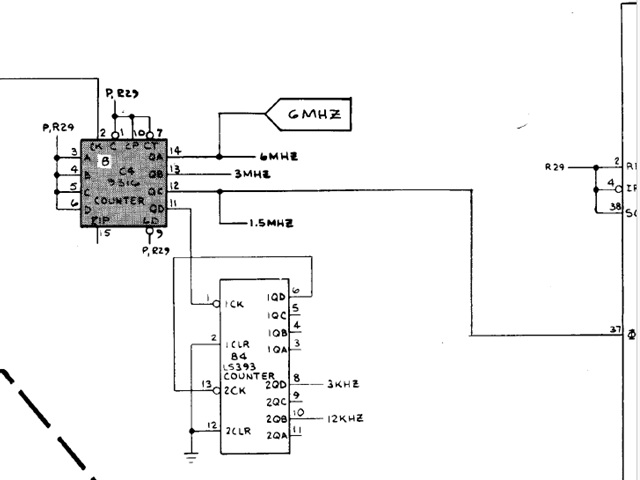
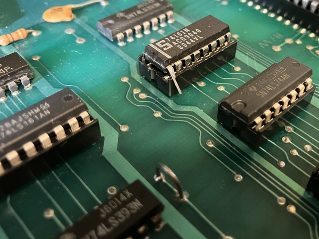
The 1.5MHz clock signal to the CPU pin 37 (seen at the right hand side of the diagram above) comes from pin 12 of the 74161 IC in position C4 which in this case has no output. In most instances I would substitute a 74LS series component but referring to the Atari Asteroids circuit diagram it appears a 9316 counter IC (equivalent to an original 74 series TTL IC) has been specified rather than a 74LS component. The shading of this symbol on the circuit diagram denotes a circuit revision.
The adjacent NMI counter in position C5 is a 74LS161 which confirms that Atari deliberately selected two different IC types for these positions, most likely due to the higher output current rating of the 74 series over the 74LS component. Unfortunately I have no 74161s on hand at present so have ordered some from a known seller of New Old Stock TTL ICs and will need to wait for those to arrive from overseas.
Meanwhile, removing the 74161 to install a socket for its replacement I have found an inconsistency between the meteor PCB and the Atari Asteroids circuit diagram. Having removed the IC I can now see a number of connections which are shown on the diagram are not present on either side of the PCB. Although this may not have caused the clock divider to fail it could be a clue to the other crashing problems which I was previously tracing.
In the circuit diagram above it can be seen that a number of pins of the counter / divider IC C4 are held in the logic High state via a pullup resistor R29. Although an unused TTL input would normally default to the high state that would leave the input vulnerable to interference or crosstalk from nearby signals, especially where high frequency signals or lower power 74LS series components are involved.
Tying a TTL input directly to the +5V Vcc rail is not recommended as inrush currents at the input during initial power on can damage the IC internally so an added resistance is recommended (if an input needs to be tied to a logic low state a direct connection to ground is acceptable). Ideally an individual pullup resistor (say 10k Ohm) could be added to every input which needs to be held 'High' but in this case a single 1k Ohm resistor is used for several inputs.
According to the Atari circuit diagram R29 appears to connect to ICs C5 pins 5 and 7, C4 pins 1,3,4,5,6,7,9 and 10, D4 pins 4 and 13, CPU pins 2,4 and 38 also 2 inputs of the multiplexer IC K3, pins 6 and 10. Tracing the connections on the Meteor PCB however there is no connection from IC C4 pin 3 to pins 4,5, 6 or 7 leaving 4,5 and 6 floating. That's not too serious as those are unused parallel load inputs.
Of more concern; that also leaves C4 pins 7,9 and 10, CPU pins 2,4 and 38 also K3 pins 6 and 10 still connected together but no longer pulled high by R29. That is most likely a 'bootleg' error where a copy has been made from an original Asteroids PCB and some connections have gone unnoticed. Those inputs have effectively been left to collectively float high. In the photo below I have added a wire link to restore the connection to the previously isolated group.
Confirming the connections with my multimeter the noted inputs now all show continuity to R29 and a 1k Ohm reading from the +5V rail. My order for some old stock 74161 counter / divider ICs has just arrived so after first testing them using my EPROM programmer's IC test function it's time to install one into position C4 and see where we stand.
Well, the clock signal seems to run briefly then stop. Using my oscilloscope to check the outputs of the 74161 there is a burst of activity at power on then nothing. Checking the other pins of the IC there seems to be an issue with the inputs which are pulled high by R29 now sitting at just over 1 Volt, in the undefined region between a logic High or Low.
Perhaps joining that signal to the previously isolated inputs has added some excessive load but as far as I have been able to measure the circuit now matches the Atari diagram and should work as intended. Unfortunately as R29 connects to multiple inputs across a number of ICs it's not straightforward to trace which exact point is loading the circuit.
From the perspective of the design engineer the pullup resistor is a formality and combining the need to tie multiple inputs High to a single resistor makes perfect sense. The nominal load from each is minimal so a 1K Ohm resistor is sufficient to ensure multiple inputs remain in the logic High state. On the Asteroids CPU PCB there are only two, 1k Ohm pullup resistors for the whole board.
In the opinion of a service technician that is a disastrous approach for this exact reason. A single faulty input on one IC can increase the load across the pullup resistor to the point where widespread parts of the circuit behave in an abnormal manner making fault tracing far more difficult. If a separate pullup resistor was used for each IC then it would be a simple task to identify the faulty component.
I don't like the practice of cutting and rejoining tracks or IC pins to locate a point which is shorted or drawing excessive current, in these situations I prefer to remove and socket ICs which minimises damage to the PCB traces and makes troubleshooting easier in the long run. Only if specific ICs are very rare, expensive or irreplaceable would I avoid disturbing them at all.
So I have removed each IC which connects to R29 in turn, adding a socket and measuring the Voltage at the pullup resistor with no IC installed or with a new IC substituted. Each time I expected to eventually locate the point which was loading the circuit but after trying every other IC the only remaining possibility was an issue around the CPU itself. I had already replaced the old CPU and its socket and tested the 'new' 6502A CPU in an external tester to confirm it was working correctly.
Nonetheless, if I power the board up with no CPU installed and measure the Voltage at the pullup resistor it is correct at nearly +5 Volts but falls to around 1 Volt with the CPU installed in its socket. Substituting another CPU IC also makes no difference. I have checked for shorts between any pins of the CPU socket and found none. At this point I'm reminded of a phrase attributed to Arthur Conan Doyle's Sherlock Holmes which appears in numerous titles with slight variation;
'When you have eliminated the impossible whatever remains, however improbable, must be the truth' (The Sign of the Four by A. Conan Doyle, 1890). Could there be some conductive residue on the PCB under or around the CPU socket? I haven't been able to identify such a problem with my multimeter but can't think of any other possibility at this stage. That could also explain the strange address buss crosstalk I mentioned earlier.
Looking back, I recall the circuit was working fairly well with only occasional crashes and noted that pressing lightly on one end of the CPU caused it to crash. That was almost certainly due to the old single-wipe IC socket so replacing that was the obvious solution but the non-starting or continuous crashing issues all seemed to occur after that point so maybe I have introduced a new problem.
I don't use any flux when removing or replacing through hole components as a rule and generally use a suction desoldering tool rather than solder wick when cleaning out the pads. Before fitting a new component or socket I usually clean the component side of the PCB with some Electronic Cleaning Solvent and a small cotton bud and after soldering clean the residue from the solder side with cleaning solvent or alcohol and a small brush.
That process has never failed me in the past but I wonder if this particular PCB had some non visible, conductive residue under the CPU socket which I may have inadvertently spread over the pads before soldering in the new socket. It does seem unlikely but might explain the present symptoms.
My latest setback with the Meteor PCB repair is the main clock signal divider IC not running due to a control signal which should remain high but doesn't. A number of inputs are tied to the +5V rail via 1k Ohm resistor R29, the Voltage at that junction is being loaded down to around 1 Volt due to some current drain. I haven't been able to measure any current path directly to ground so either a faulty input on a connected IC or a PCB short circuit to some other signal must be responsible.
So far, I have removed and socketed any ICs which connect to R29 on this PCB, testing with each IC not present or a new working component fitted and no difference to the fault symptom which leads me to suspect a PCB short. I've checked for a low resistance path from R29 to any other pin on the socketed ICs but haven't been able to identify any obvious issues.
As a precaution I'll go ahead and give the PCB a thorough clean on both component and solder sides, I never wash PCBs with water or in a dishwasher due to the long term deterioration that may cause but after removing newly socketed ICs I'm cleaning the entire area with a made for purpose product called Kleanium before rinsing with alcohol and blowing with compressed air.
Not surprisingly that hasn't provided any miracle cure so back to circuit tracing; I'm thinking if I remove the link which I previously added from IC C4 pin 3 to pins 4,5,6 and 7 then remove ICs C4, C5 and D4 from their sockets as well as lifting one side of R29 that PCB trace should be entirely isolated with no connection whatsoever. If I do that and then measure on a high resistance setting even the slightest connection should become apparent.
But wait, what's this? Something I have been missing all along - there is a trace which ran directly under R29 which I didn't notice. I've now followed it to the inter board connecting ribbon cable and found some more, previously unnoticed connections from R29 to ICs in positions A7, B7, C7, D7 and A9. It seems ridiculous to carry a signal from a pullup resistor across to a separate PCB but of course the Atari board was a single PCB so the connection was more or less direct in that example.
All the same, it's still a long way removed from the CPU clock area to carry a signal to a completely separate part of the circuit just to save the cost of an additional resistor. This section is the vector timer which counts the time to draw a vector before moving on to the next and appears on a different page of the Atari circuit diagrams. Of course if one of these ICs is faulty it could affect the function of every other IC which connects to R29.
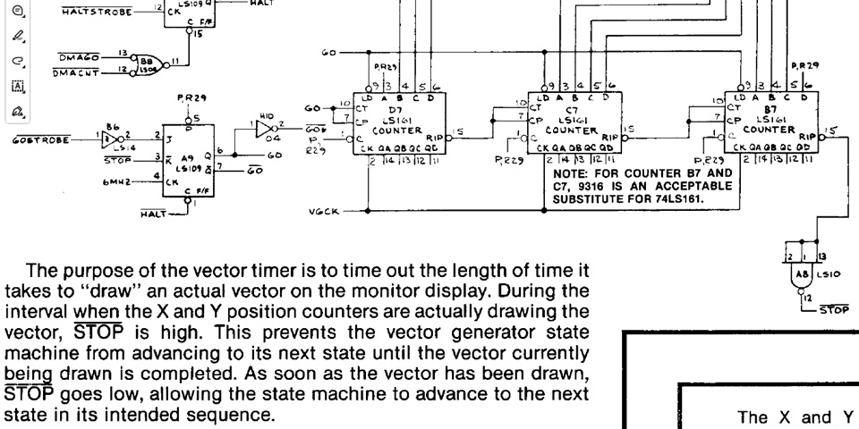
Now to determine which if any of these ICs is causing the current drain on R29; it's difficult to trace an issue when there is no activity due to the clock divider IC C4 not operating. That's due to its /Clear input pin 1 not being pulled high by, you guessed it - R29. So instead I'll just carefully bend its pin 1 away from the socket allowing it to float high and the clock is now running. Lets take some measurements to see if we can identify a faulty IC.
With pin 1 of the clock divider IC C4 floating high the CPU clock now continues to run regardless of the state of the signal at the junction of R29 so my little test program is running where it previously was halting when the clock stopped. That makes an interesting change as there is now a stream of pulses showing at R29 rather than a steady 1 Volt level.
That's obviously still not correct as the signal should be a steady logic High but does confirm that there is some connection to another signal either due to a faulty IC or some short across PCB tracks. As the fault was not present all along I'm still inclined to favour an IC fault and now have five new suspects to investigate. Looking at the signals around the counter ICs I have found one output of IC D7 which seems to correlate exactly with the pulses showing at R29.
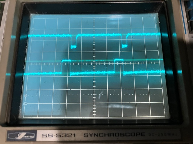
The top trace shows the signal at R29 which also appears at D7 /Clear input pin 1. The lower trace shows D7 output pin 11 but I'm not sure whether this IC is causing the faulty signal or just responding to the signal at its /Clear input. For want of a better alternative I will remove the IC and install a socket, see if the symptoms change:- Unfortunately that does not alter the spurious pulses at R29 so the number of suspects is now reduced to four.
Speaking of which, the fourth remaining IC which is not shown in the diagram above is a 74LS74 D type flip flop in position A7. In the Atari circuit diagram it's not clear whether its unused /Clear inputs are tied high via R27 or R29 but I have confirmed on the Meteor PCB both input pins 1 and 13 connect to R29. Also on the Meteor PCB the connection from pin 4 to IC R8 pin 6 is not present, pin 4 of A7 is also connected to R29.
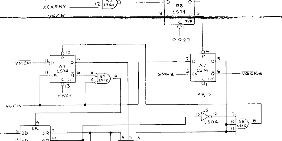
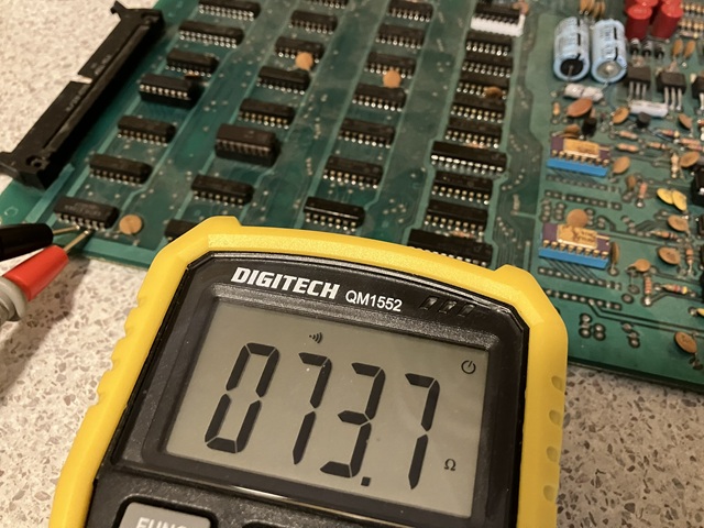
With 3 connections to R29, I'm inclined to test for any short circuits or low resistance paths to any adjacent pins of IC A7. I tried this test previously with ICs on the CPU PCB but not in this section as yet - and finally that impulse pays off! I have found a low resistance of around 74 Ohms between A7 pins 13 and its D input pin 12. Even when I snip pin 12 to disconnect it from the PCB the low resistance can still be measured across those two IC pins.
So, after replacing the 74LS74 in position A7, adding a socket as usual the problem with the spurious level and signal on the pullup resistor R29 is finally resolved. That returns the CPU clock generation to a working state although previously experienced crashing problems still remain to be solved. The use of a single pullup resistor for such a wide area of the overall circuit certainly did not help with diagnosis of the fault symptom in this instance.
I have been coming back to the repair of this Meteor, Asteroids clone PCB when time permits and have made considerable progress only to be more or less back where I began, with a non working PCB set. Initial faults confirmed and corrected so far include a faulty Voltage regulator IC and Zener Diode, 2 x inductor with broken leads, 2 x 2114 RAM memory IC, 2 x rusted 4066 CMOS analog switch which have been replaced along with their IC sockets.
At that stage the game was up and running albeit with some intermittent crashing and sound issues. Replacing the CPU socket and the CPU itself appeared to have corrected the intermittent crashing until, after a few hours of testing the board stopped working altogether. This appears to be an unrelated, secondary fault which has occurred rather than a recurrence of previous issues.
While tracing that problem which seems to relate to the integrity of signals on the CPU address bus a second, secondary fault (should that be referred to as a tertiary fault?) occurred which was preventing the CPU clock signal from operating. After considerable effort I traced that issue to its cause, replaced a faulty 74LS74 IC to restore the function of the clock signal.
Which brings me back to the first, secondary fault which is yet to be resolved. I have made progress, testing components out of circuit as well as developing some 'homebrew' test programs to confirm the function of CPU, memory and surrounding logic within the PCB. Checking signals with my oscilloscope as the test programs ran showed several waveforms with irregular shape and marginal logic levels, especially around the buffered CPU address bus.
The address and data buffering has two tiers for access to program as well as vector memory with the complete circuit spread over two pages of the Atari schematic diagrams so I drew up a block diagram to simplify the process of fault tracing. My original hand drawn sketch has been very helpful but too messy to reproduce here so I have taken the time to redraw it as below.
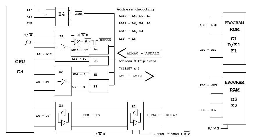
The 6502 CPU has no internal buffering of its outputs, each having a rated fan out of 1. That is, each output can only drive a single TTL input or equivalent load so external buffering is essential even on the smallest computer system. In this instance a pair of 74LS244 buffer ICs handle the 16 bit address bus while a single 74LS245 carries the bidirectional 8 bit data to and from program memory, 6k Bytes of ROM and 1k Byte of RAM.
A second 74LS245 data buffer and 4 x 74LS157 address multiplexers, when enabled allow the CPU shared access to the vector memory being 2k Bytes of ROM and 2k Bytes of RAM. Apart from address bits A0 to A12, the Read /Write signal and CPU clock phase 2 are buffered to control multiple devices. Address lines A13 to A15 are not buffered and only used for address decoding by the 74LS139 in position E4.
The initial address decoding by IC E4 divides the 32k Byte address range into four blocks comprising program RAM, I/O devices, Vector memory (ROM and RAM) and program ROM. The upper 32k Bytes of the full 64k address range is unused. Buffered address lines AB9 to AB12 are used for further address decoding to select individual memory and I/O devices.
My main concern at this stage is the integrity of the buffered address bits AB0 to AB10 which are used to access program instructions from ROM. When my test program was running the waveforms on the address lines looked quite irregular with steps in the Voltage levels suggesting some crosstalk from other signals. The most likely cause would be the 74LS244 address buffers in positions B2 and C2 but removing those, fitting new ICs and sockets made no difference to the symptoms.
I've been trying to solve a CPU crashing problem with the Meteor PCB which seems to be due to marginal signal integrity between CPU and program ROM. So far I have been concentrating on the buffered CPU address bus which is showing some irregular logic levels apparently due to crosstalk between the signals of the individual address bits. By comparison the data bus signals appear fairly normal with consistent levels.
To pinpoint the cause of the program failure I'm trying to isolate the main components which are critical for the CPU to run a program. This includes the CPU clock signal as well as program ROM and RAM, address and data buffering and address decoding. Referring to the block diagram above, secondary parts of the circuit are accessed via address multiplexers in positions F3 to K3 and a secondary data buffer in position R2 on the PCB.
In an effort to eliminate the address multiplexers as a possible cause of the address line crosstalk I will remove and socket those 4 ICs. By also removing the secondary data buffer from position R2, which is already socketed the main CPU area is now isolated from the rest of the circuit. Running my simple test program once again, the address crosstalk is amazingly still visible, suggesting that anomaly is caused by the PCB itself.
It could be the track layout with address lines running parallel over long distances or some conductive residue which remains after several cleaning operations. Either is possible as the Atari PCB layout did include an option for different ROM types with a row of unpopulated IC positions having address and data lines running parallel from each position to the next.
On this particular PCB, being a bootleg or clone of the Atari circuit the PCB itself appears to be of a lower quality with a fairly dull apearance and rough texture of the solder mask. When rinsing with alcohol the PCB gave the appearance of being porous so it is entirely possible that some residues remain even after cleaning.
That doesn't prove that the irregular levels on the address bus are actually causing the program crash. Any signal between 2.4 and 5.25 Volts is considered a valid TTL logic High so a considerable variation in the logic high level is tolerable. The logic Low levels are more critical but the signal lows do appear to remain within the range from 0 to 0.8 Volts which are also valid for TTL logic Low.
Looking for any other potential cause of the program crashing I'm turning my attention to the Data bus once again; with the test program running and secondary buffer R2 removed from circuit the data levels and transitions on both sides of the main buffer look OK. On the EPROM side there is some signal inbetween logic low or high, this is expected 'bus idle' time while the CPU is performing internal operations the Read/ Write control signal remains high although neither ROM nor RAM is selected.
In this case there is a bank of pullup resistors added to the data lines so the bus idle signal appears as a sort of sawtooth waveform. Checking the buffer inputs and outputs of the 74LS245 from pins 2 to 9 and 11 to 18 I can't see any obvious problems. Pin 1 controls the buffer direction, driven by the buffered R/W signal. Pins 20 and 10 are +5 Vcc and ground, pin 19 is the tristate enable or /G signal - but what's this?
I'm measuring just over 1 Volt on pin 19 which is not a valid logic low. The buffer is passing signals but I wonder if this invalid logic state on its enable input may be causing intermittent dropouts and crashing the CPU - it's definitely possible. Pin 19 is supposed to be connected to ground meaning the buffer is always enabled so what has gone wrong?
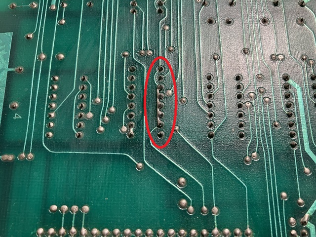
Using my multimeter to check for continuity from the ground track to pin 10 of the buffer IC confirms a good connection but measuring the interconection from pin 10 to pin 19 returns a high resistance reading. So the track which joins these two pins on the component side under the IC socket must be damaged. Looking back, I did remove and replace the original single wipe IC socket with a new dual wipe socket but this was after the CPU crashing problem had arisen.
Usually when replacing an IC socket I will test continuity from each IC pin to its corresponding PCB pad but most likely did not confirm the connection between those two pins or notice any visible damage with the socket removed. So it's not clear whether there was already a problem with that track prior to replacing the IC socket but it certainly could account for the onset of the CPU crashing fault.
Looking at the solder side of the PCB footprint for the data buffer, there are two sets of pads to allow either of two IC types to be used in this position. It turns out the connection from pin 19 to ground at pin 10 is not direct but passes from the component side to solder side and back again via two PCB pads with plated through holes. It could be the bad connection was due to a problem with the hole plating, either way I have added a short piece of wire to bypass the poor connection.
I also replaced the two single wipe IC sockets for the program RAM, experiencing one lifted pad on the component side. Although the connection measured OK I added a wire from pin 16 on the solder side to the nearby via to bypass the damaged area. I have been taking great care not to damage PCB tracks or pads but have found the quality of the pads to be especially poor with a very small surface area and holes drilled slightly off centre making it difficult to achieve a neat solder joint.
Anyway, with the poor track connections repaired the test program now runs reliably, the CPU /RESET signal from the watchdog timer remaining high. The next step will be to install the four 74LS157 multiplexer ICs into the newly fitted sockets, refit the 74LS245 buffer to position R2 and return the ME1 EPROM to the boot ROM position C1 to see if the CPU crashing problem has been resolved.
To be continued...
Meteor / Asteroids specifications
| Made | 1979 |
| CPU | MOS Technology 6502A @ 1.512 MHz |
| RAM | 1k Byte program RAM plus 2k Bytes vector RAM |
| ROM | 6k Bytes program ROM plus 2k Bytes vector ROM |
Web Resources (External Links) -
Hamster's Online Rom identification
All images and text on this website are Copyright.
Contact: jbtech at telstra dot com