Apple - 1 reproduction
This is likely to become a long term project! Having previously assembled an almost exact reproduction of my first computer, the Ohio Scientific OSI600 Superboard II from 1979 and a replica of the Sinclair ZX80 from 1980 (with a couple of modern component substitutions and even a 3D printed replica plastic case) I began thinking about another vintage computer project.
Reproducing an original PCB is possible and open source PCB files already exist for several early computers but the plastic or metal cases are not so easy to accurately replicate; fortunately the ZX80 case was small enough to make a 3D printed option viable and open source files already exist for those as well. For the next project, an early computer which was available in PCB only form would be the simplest option.
Reading some advertisements from around the time of my original Superboard II, I did notice even Apple II computers were initially advertised with a PCB only option. Researching around that I stumbled upon some mentions of the computer which preceded it, the very first Apple computer model 1 from 1976. Up until this point I was not familiar with the Apple-1 story, by the time I became interested in home computers (around 1980) the Apple II was already well established - but beyond my budget at the time.
As only a couple hundred Apple-1 computers were ever produced and very few original units survive, their value as the landmark product which launched a global computer corporation has soared into the million dollar region. This seems like a perfect subject for a reproduction project, a rare, milestone computer with an interesting back story and original units well beyond the means of ordinary computer enthusiasts.
So the good news is the Apple-1 PCB has already been accurately reproduced with blank boards for sale online as well as open source PCB files freely available. The bad news is many of the components originally used are becoming almost unobtainably rare and expensive in their own right. I'm not too concerned with producing a museum style reproduction which appears identical to an original unit but will aim for a functionally correct, working computer and may need to substitute a couple of the rarest components with more readily available parts fitted to small adapters where required.
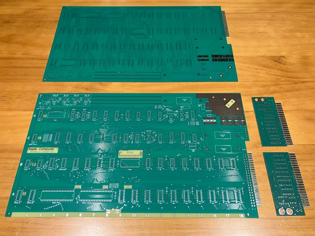
The first step will be to source the PCBs for the Apple-1 as well as its 'optional' cassette interface; a number of these appear to be available online but none locally so the second option of having a small batch produced from open source PCB files seems more attractive. I found the necessary gerber files for the PCBs via the applefritter website (link below) but am not sure who it was that took the time and effort to reproduce the Apple design and share the files originally - my thanks go to them, anyway.
Sending the files off and opting for a basic HASL (Hot Air Solder Levelling) finish - simply means exposed contacts such as the expansion edge connector will be tinned rather than gold dipped or plated. Once again, I'm not so concerned with the unit appearing identical in every respect but do want the finished computer to resemble the original Apple-1 design and layout where possible. Once ordered, the PCBs were completed and arrived without delay. The project is now officially underway!
The PCBs look great! From the photo above one detail I have neglected to mention up until now would become clear - no keyboard is included with the computer, a separate keyboard with parallel ASCII character output was required. Once the computer itself shows some signs of life, sourcing or constructing a suitable keyboard will be the next issue.
Apart from that, two external transformers are required to provide the AC secondary Voltages for the on board rectifiers and DC Voltage regulators. The Apple-1 uses multiple Voltages (and even differing logic levels) throughout, unlike my previous projects which were able to work with a single +5V supply and TTL logic levels. So begins the task of sourcing the required components...
I've made a start on my latest vintage computer reproduction project, the Apple-1 from1976. The PCBs are here and I've begun ordering components, sifting through my existing spares for some of the more common parts and highlighting the critically rare ones which I will need to find or otherwise seek alternatives. The video terminal section in particular uses some now very scarce components:
Signetics 2504 - 1024 x 1 bit dynamic shift register - Qty.7 required. I've ordered some AM1404APC equivalents, hopefully these will be genuine and not 'faked' ICs.
Signetics 2513 - 64 x 8 x 5 character generator -This seems quite elusive but is basically just a character ROM; I've made up an adapter to substitute a 2716 EPROM.
Signetics 2519 - Hex 40 bit static shift register - I've found an open source design which substitutes 6 modern single bit shift registers with a small adapter PCB.
I'll begin by fitting low profile components such as resistors and signal diodes then IC sockets before capacitors and larger components but won't fit the ICs themselves until the power supply section has been completed and tested. In the photo above I've test fitted the adapter PCBs for the 2513 character generator and 2519 shift register which plug into the IC sockets fitted to the main PCB.
I'll include links to the adapter information below. In the case of the 2513 I did find a couple of existing adapter designs, the first seemed to have a few connections missing for example the Vpp pin of the 2716 EPROM is normally tied to Vcc rather than left floating during read operation, also the ground connection from the 2513 footprint to the 2716 seemed to be missing.
Another 2513 adapter designed specifically for the Apple-1 included protection diodes on the 2716 address inputs to cope with a negative Voltage logic level from the original 2519 shift register. In this case however I'm not using an original 2519 so the 6 x 7.5k Ohm pull-down resistors which connect to the -12V rail can be omitted instead. So I've made my own simple adapter from the 2513 to 2716 EPROM pinout.
The 2519 adapter meanwhile uses 6 SMD shift registers (2 on the underside of the PCB) and spans across to the otherwise unused IC socket in position C1 - mainly for stability although the ground connection from that position is also used. The 7k5 resistors which I'm omitting are normally positioned in the space between sockets C1 and C2. The SMD components on the adapter look out of place amongst the mid '70s tech but needs must...
If I ever managed to source the two rare Signetics components the PCB could easily be returned to original configuration by unplugging the adapters and fitting the pull down resistors to their original positions so the modifications in this case are completely reversible.
Another component which has become scarce and expensive is the DS0025 clock signal dual line driver IC. In this case I'm ordering a slightly faster, pin compatible DS0026 so will test that component in circuit and check the waveforms before fitting the shift register ICs. So once the power supply section is complete the process of populating and testing the circuit will need to be done in stages beginning with the main oscillator and timing circuits.
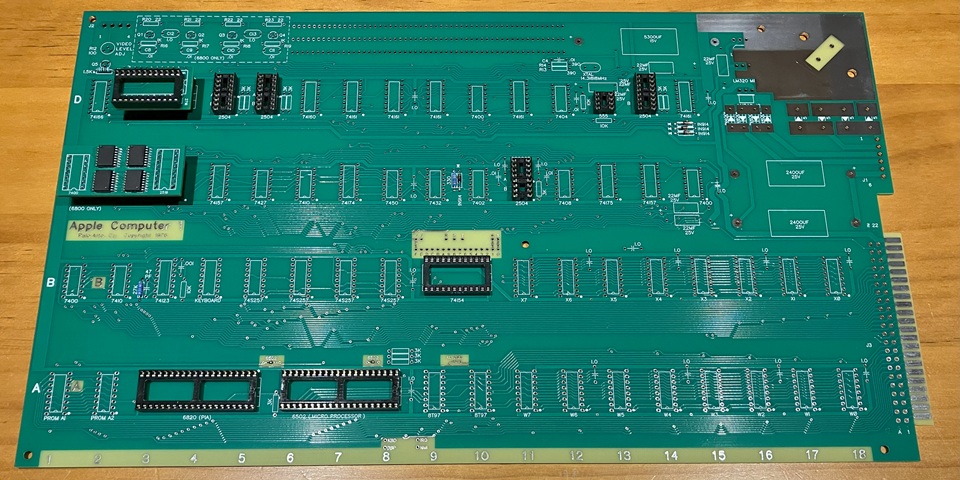
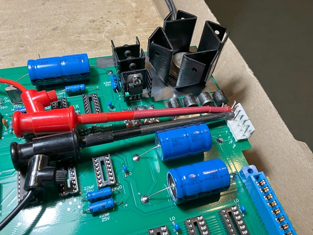
I'm building up a reproduction of the Apple Computer 1 PCB and so far have fitted all of the IC sockets as well as most of the passive components and connectors for power, video as well as the edge connector for the all important Apple Cassette Interface (ACI). The next step is to complete and test the power supply section to ensure all of the Voltages are correct before adding any of the logic components.
The power supply is conventional '70s tech with linear, 3 terminal regulator ICs providing the 4 Voltage rails required by the components of the day. Most of the parts or equivalents are readily available, the main issue will be sourcing the LM323 5V 3A regulator in TO-3 package which seems to have no currently produced replacement. As a result, New Old Stock (NOS) components are now highly sought with increased prices and the emergence of many 'faked' examples on offer.
It seems a faked component is usually some similar looking but less valuable item which has had its part number scrubbed off and is then rebranded with the markings of a rare or highly valued component. Often the fraudulently substituted item may be a pin compatible but lower spec. component which may work in some situations but most likely will not be suitable and fail prematurely or not work at all.
Searching on line for this particular component, I have avoided a few of the very cheapest examples on offer which all seem to bear identical markings and settled upon one which appears correct and is 'guaranteed 100% genuine'. That is slightly reassuring as most of the worst suppliers would probably avoid that topic altogether and at least ensures that a refund may be obtained if the parts turn out to be no good.
I've ordered two, just so I have a spare if they are OK. Upon arrival they seem to look right, there are some marks on the legs and case which would seem to indicate they are used and have been screwed into a TO-3 socket but the legs have not been cut or soldered. To ensure these parts are working and meet their Voltage and current ratings I will give them a quick test on the bench before installing one into the apple-1 PCB.
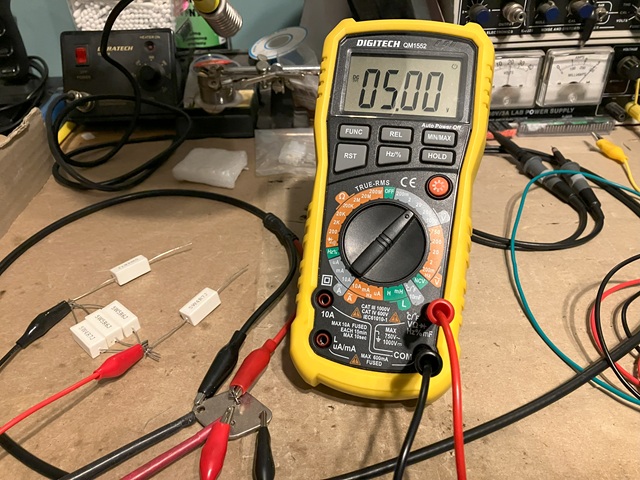
Using my bench power supply set to around 10V, connected to the IC input and measuring the output with my multimeter the output reads 5 Volts. So far, so good. Now placing some 4.7 Ohm and 5.6 Ohm resistors in parallel across the ICs output to ground I can view the current drawn on my bench supply current meter. Each resistor should draw around 1 amp at 5 Volts and dissipate about 5 Watts of power.
Adding each resistor in turn I can see the IC output remains at 5V each time with current increasing in steps from 1A to a final 3A which can just be seen on the power supply current meter in the background of the photo above. It's a brief test as the load resistor bank and the IC are dissipating about 15 Watts of power each and get hot quickly without a heatsink but a lesser component would have shut down immediately so this one does appear to be a genuine, working IC.
Unfortunately when I similarly test the second IC there is virtually no output Voltage, measuring about 0.9V. I'm fairly sure these are both correctly labelled ICs but the second one is faulty. They are obviously not new or N.O.S. components, most likely recovered from some old equipment and probably untested prior to sale. At least I do have one working component to use with this PCB so will move on.
Here's the project as it stands. I'm sure I will be upsetting some of the purists with my component choices for the power supply section as I haven't scoured the surplus stores for the humongous, 50 year old Sprague capacitors fitted to the original computers - instead using some current production stock with slightly increased preferred value capacitance and Voltage ratings.
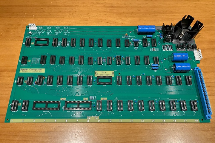
I can't help imagining that Sprague, back in the day rolled up some electrolytic capacitors to a convenient size (for the time) then measured them to work out what capacitance they ended up with... So, instead of 5300uF at 15VDC rating I'm using a 6800uf 25V 105 degree component and for the 2400uF 25V originals I've substituted a pair of 3300uf 25V axial caps. Are they smaller or larger? That depends on how you look at it.
And the sacrilege doesn't end there; instead of the finned aluminium heatsink for the +5V regulator I've used a low cost / high efficiency product which outperforms a lot of the more expensive finned designs. I've also added small heatsinks to the three TO-220 regulator ICs which apparently weren't present on original computers. So it looks a bit different but should work well.
I've added the power supply components to my Apple-1 reproduction PCB so can test the Voltage rails before I begin to populate the crystal oscillator and timing circuits. I have two transformers which should be suitable to power up the PCB when required but in the meantime can just use my trusty bench power supply to check each Voltage regulator one at a time.
Beginning with the +5V rail and setting my supply to 10V DC, connected to the input pins 1 and 2 of the power connector on the PCB; the current flows through 2 of the 4 bridge rectifier diodes resulting in about 8.8 Volts as measured at the large smoothing capacitor and 5.0V at the output of the LM323 regulator, measured at the supply pins of the sockets for the logic ICs. Reversing the polarity of the input Voltage gives the same result, the other 2 diodes will carry the current in this instance.
Moving on to the +/- 12V and -5V rails, adjusting the supply Voltage to 15VDC and connecting the positive lead to one of the AC input pins (3 or 4) with negative lead to the centre tap / ground pin 5 gives about 14.4V at the smoothing capacitor (lower right in the photo above) or pin 1 of the 7812 regulator with its output pin 3 reading about 12.2VDC. Next, reversing the polarity of the supply Voltage allows us to test the -12V and -5V supply rails.
Having reversed the polarity of the input Voltage we can now measure about -14.4V at the 'middle' smoothing capacitor, also at the input (centre pin, heatsink tag) of the 7912 regulator IC (also the middle of the 3 TO-220 regulator ICs) Its -12V output can be measured at the input to the 7905 regulator (heatsink tag or pin 2) with the -5V output at pin 3.
Of course with the power transformers connected all 4 power supply rails will be present at once but having tested them individually we can move on to adding some logic components. With early system designs such as this the usual caution applies about substituting 74LS components for original 74series TTL ICs. Mainly due to their lower current capability, these later ICs will often not work in place of the earlier type.
And as usual I'll be throwing that caution to the wind, attempting to get the circuit running using 74LS series ICs wherever possible. In some sections that will not be an option and I may need to use the higher current 74S type or revert to original 74 series components, we'll work that out as we go. Beginning with the crystal oscillator inverter in Position D12 I know the 74LS series would not be suitable as the IC needs to drive a capacitive load at high frequency so I will try a 74S04 instead.
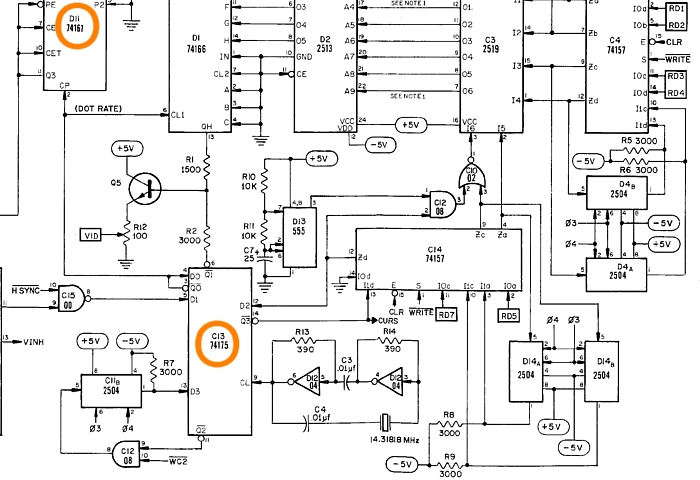
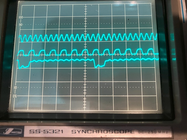
So far, so good. As I only need the +5V logic supply for the moment I'm still using my bench supply to power that up and the crystal oscillator using a 74S04 inverter in position D12 is running, the signal looking fine on my oscilloscope and frequency appears correct. Next I'll concentrate on the signal path from oscillator to timing circuits, install a 74LS175 quad D type flip flop in position C13 and 74LS161 counter in position D11.
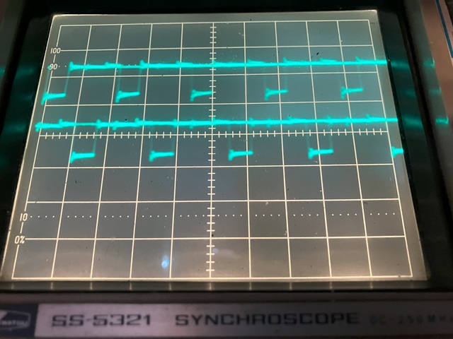
The D0 input of the 74LS175 is linked to the inverted /Q0 output causing that flip flop to toggle on each full clock cycle resulting in a 1/2 clock frequency output of 7.15909MHz. This is noted as the 'dot rate' or horizontal pixel freqency on the circuit diagram. From there the 74LS161 counter in position D11 divides the frequency with the Q3 output noted as the 'character rate' signal.
The D11 counter is set up to divide the 'dot rate' signal by 7, resulting in a 1.023 MHz 'char rate' signal, also used as the CPU clock rate. The waveforms for the crystal oscillator, dot rate and char rate signals can be seen in the 3 trace oscilloscope image below. Counting from the falling edge of the char rate signal (lower trace) at the left of screen to the point where that waveform repeats there are exactly 7 full cycles of the dot rate signal (centre trace) and 14 of the oscillator frequency (upper trace).
The 74/LS 161 is a 4 bit binary counter which will count from 0000 to 1111 in binary (0 to 15 decimal or 0 to F Hex.) although the value can be reset or preloaded to alter the count sequence. In this case the most significant bit Q3 is used as the 'char rate' signal and, when low will inhibit the count as well as preload a binary value of 1010 or decimal 10. So the count sequence is 0, 10, 11, 12, 13, 14, 15 which then repeats.
That will result in each of the 40 characters displayed across the screen occupying 7 pixels horizontally, the characters generated by the Signetics 2513 being only 5 pixels wide so each character on screen must be separated by 2 blank pixels. Moving on, I'll begin to populate the counter / divider chain which generates the video sync and other timing signals starting with ICs in positions D6 and D7.
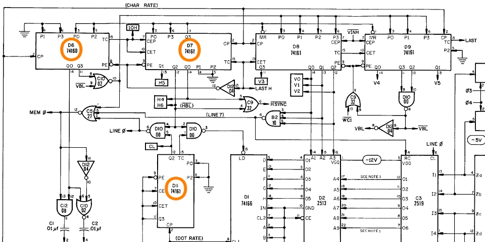
Here I've encountered my first problem; the Q3 char rate output of IC D11 connects to the clock inputs of counters D6 - D9 and I can view that signal at the CP input of IC D6 but its outputs are static with no activity. The IC I'm using is a new, 74LS160 which I've confirmed working so I suspect the issue may be due to unused inputs which have been left floating in the original design.
The input pins of TTL logic ICs have an internal pullup resistance so if left unconnected would usually be assumed as a logic 1 but later 74LS series components, to reduce input loading have a higher resistance or weaker pullup effect and are more prone to high frequency noise or crosstalk from nearby signals if left floating. In later designs it became good practice to either tie unused inputs to ground or pull up to Vcc +5V via an external resistor to ensure the correct logic level.
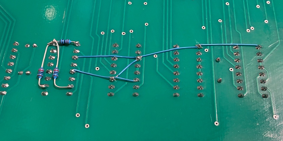
In this case the ICs /Clear input as well as the two count enable signals CEP and CET have been left without connection on the PCB. I tried touching the /CLR input with a wire connected to +5V via a 10k Ohm resistor but that made no difference so I suspect the count enable signals are also affected. I'll add a pullup resistor from Vcc, pin 16 to each of those inputs to ensure a logic 1 condition is maintained.
A single resistor from +5V connected to all 3 inputs could be used but is seems easier to add 3 separate 10k Ohm 1/4W metal film resistors which are quite small from pin 16 to pins 1, 7 and 10 on the solder side of the PCB. Having done that the outputs of ICs D6 and D7 now show activity, with that resolved I'll add the two remaining counters in positions D8 and D9 as well as all of the logic gates shown in the circuit diagram section above.
Now powering on again there is activity on all of the counter ICs and surrounding logic gates including signals for /HSYNC and /VBL (vertical blanking). To complete the sync generation circuit I'll install yet another 74LS161 counter in position D15 which combines the vertical timing signals to generate a /VSYNC signal and 74LS00 NAND gate C15 which combines /HSYNC and /VSYNC.
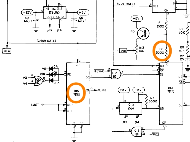
The combined sync signal from IC C15 is gated by a D type flip flop in position C13 and inverted /Q output used to restore its negative going pulse direction. From there it will be combined with video via R2 and R1, buffered by Q5. As yet there is no video signal present however the composite sync can be viewed at R2 using my oscilloscope.
I've made some progress with my Apple-1 reproduction PCB assembly having fitted all of the IC sockets, power supply components and installed ICs for the crystal oscillator and sync / timing circuits. So far I have checked for counter / frequency divider activity and observed the circuit is producing a 'normal' looking sync signal. I say normal, for a '70s computer which was only ever intended to work with a black and white CRT monitor.
There is a Horizontal sync pulse which appears to repeat at the correct interval (around 64 microseconds) according to my analog oscilloscope, punctuated by a longer vertical sync block. Setting my CRO trigger to 'high frequency reject' allows the display to trigger on the lower frequency vertical sync which appears at roughly the correct 16 millisecond intervals.
That would seem to be 'close enough for Retro' but the real world test will be whether my test bench TV monitor can lock to the sync signal and display (at this stage) a blank video screen. Installing the video output transistor then making up a cable from the video output connector to my monitor's composite video input; powering on my monitor does not respond to the sync signal and displays its default blue screen background.
Yes, it's a more modern colour TV with AV input and not even NTSC standard, it's actually a PAL standard TV but usually has no trouble displaying a 60Hz monochrome or RGB source such as arcade PCBs, other retro computers even early black and white video / TV games. I'm wondering what specifically is wrong with the signal that prevents my monitor from syncing to it.
At this stage there's no video information at all so the signal just comprises sync pulses and 'black level'. The only obvious issue with the timing seems to be the horizontal sync pulse is longer than expected, taking about 10us of the total 64us horizontal period instead of the standard 5us sync pulse duration. The total horizontal blanking period is usually around 12us including sync, front and back porch with an active video period of 52 microseconds.
So, looking around the area of the horizontal counters in positions D6 and D7 I've noticed some signals with unusual levels. These are some of the preset inputs and according to the circuit diagram are driven by output Q3 of IC D7 but checking the actual circuit none of the connections from Q3 are present. The inputs which appeared to have incorrect levels were just floating.
My first thought is perhaps the open source PCB files which I used were some early revision which may have been incomplete. In any case leaving all of those inputs floating could be an issue, especially with my choice of 74LS series counters so I'll try adding the connections as marked on the circuit diagram. In the photo below the connections have been made with fine wire, the 3 pullup resistors previously added to IC D6 can also be seen.
Having done that, powering on again the resulting signals appear unchanged. Checking the signal from the Q3 output, pin 11 of the D7 counter it appears to remain high with no activity apparent so the associated inputs are all driven high whereas before they were floating (and assumed to be read as high). So what was the purpose of these connections which were included in the original circuit diagram?
My guess is it was a startup provision; at power on if the counter outputs were at zero (or any point where Q3 of D7 was zero therefore outside of the desired count sequence) the preset inputs of the horizontal counters D6 and D7 would be set to zero, in addition the vertical counters D8 and D9 would be reset. Once the counters reached their intended sequence Q3 of D7 would be a logic high and the preset inputs of D6 and D7 would then be 0101 (decimal 5) and 1001 (decimal 9) respectively.
In practice a startup preset of the counters was probably unnecessary as whatever value they began with, they would quickly reach their intended range and settle into the intended sequence within milliseconds. After some reading I did find some hardware information on Mike Willegal's website (link below) which confirmed that these connections were also not present on the original Apple-1 PCBs
In this instance I think it's preferable to leave my added wiring in place rather than have those 6 inputs floating without any connection. But that doesn't solve my test bench monitor's rejection of the Apple-1 sync signal. So what next? After some more research I found an article and easy to implement modification by UncleBernie on the Applefritter web site (link below).
The article confirms the unusually long horizontal sync period as well as the lack of any horizontal pulses during vertical sync, are both normal behaviour for the Apple-1. To address both of these issues UncleBernie has come up with a small modification which takes the /HSYNC signal from the output of IC C9, inverts that and adds it back in to the composite video / sync signal at R1 / R2.
By carefully matching the (inverted) amplitude to an equivalent black level and shortening the positive pulse using a selected R/C value the added signal effectively extends the front porch area of the video signal and shortens the horizontal sync pulse accordingly. During the vertical sync block, the added horizontal rate pulses help to keep the monitor's horizontal oscillator on frequency and more closely resemble a 'proper' video signal.
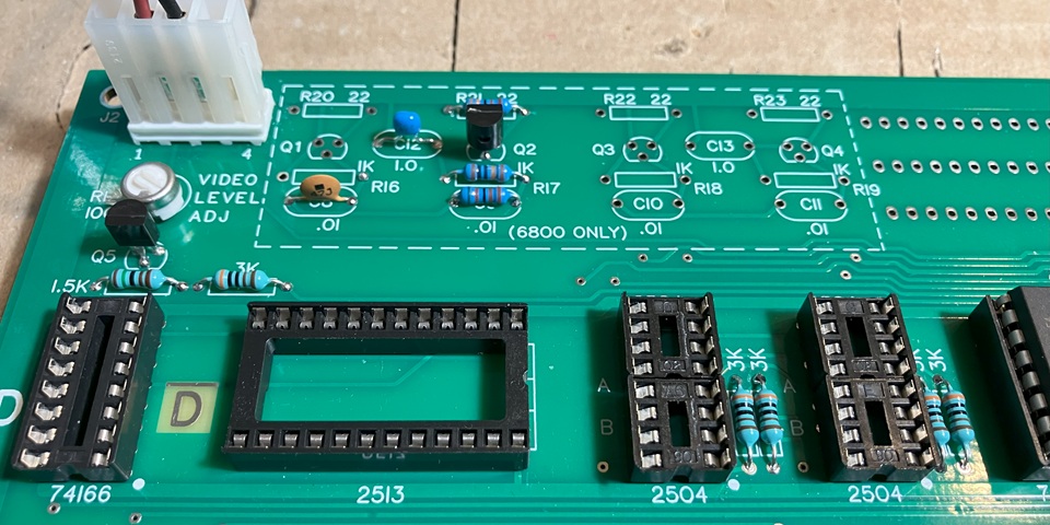
The modification involves the addition of a single transistor with a few carefully chosen resistors and one small capacitor. Although the entire mod can be added to the solder side of the PCB without cutting or modifying any traces, I have noticed a small area close to the video output section which is only intended for use with a 6800 CPU and normally unpopulated when a 6502 CPU is installed.
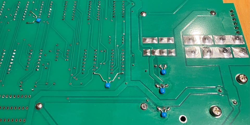
The area around Q2 has empty spaces for the required components and only needs two small track cuts on the solder side of the PCB to repurpose this area for the video / sync mod. Apologies to the purists, once again. I've also fitted the 0.1uF monolithic capacitor in position C12 which is just a decoupling, noise filter capacitor between the +5V rail and ground.
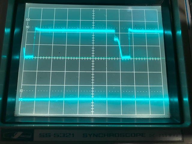
To complete the modification I've added fine wire connections from IC C9 Pin 6 (actually from the nearby via connected to that signal) to the open side of the capacitor (marked C8 on the PCB) and from resistor R21 to the R1 / R2 junction. And it works! Powering back on, my monitor now detects the sync signal and displays a stable, blank screen.
Looking at the video output with my oscilloscope I can see the horizontal rate pulses now present during vertical sync. Changing the timebase to zoom in on the horizontal sync we can see the extension of the video line and shortened sync pulse of around 6 milliseconds duration. At the moment there's an amplitude mismatch between the video 'black level' and the extended front porch area just prior to horizontal sync.
That's most likely because no video components are installed as yet so the other side of R1 is floating rather than connected to the output of IC D1. I'll check those levels again once the video hardware is working and adjust the value of R21 if required. So the next step will be to work on the video section beginning with the clock driver for the video shift register ICs.
My Apple-1 reproduction PCB project is beginning to take shape; so far I have populated the power supply section and sync generation part of the video terminal circuit. In case anyone is interested which ICs specifically are required for this section to run, I have installed ICs D6 - D12, D15, C9, C10, C13 and C15 as well as all of the discrete components i.e. resistors, capacitors, diodes, crystal and video output transistor Q5.
I've also fitted ICs B2, C5 and C12 which are shown in the same part of the circuit but don't appear to affect the sync timing. They are used to create the clock phase 3 and 4 signals which control the video shift registers via clock driver IC C11a. This area will require some extra attention as I hope to substitute a more readily available and less expensive DS0026 clock driver for the originally used DS0025.
The two ICs are pin compatible and the DS0026 has higher speed and output current ratings however those are not always advantageous as the clock signals could be prone to overshoot or ringing and may also induce more noise onto the power supply rails. To begin with I'll add the DS0026, leaving all of the shift register positions empty then add just one of the AM1404 APC shift registers to the 'cursor' position, C11b.
I'm fairly confident that the DS0026 ICs which I have bought are genuine though I have read about the much rarer, more expensive DS0025 being widely faked. Some 'fake' ICs might be a pin compatible alternate part which may or may not work in a given situation while others may be a completely different component, only bearing an external resemblance to the genuine item. In the case of these two parts there is a simple check which may help to identify a fake component.
Both the DS0025 and DS0026 have an internal pull down resistance from each input pin (2 and 4) to V- pin 3. They can be measured with a multimeter and should be around 250 Ohms for the DS0025 and 10k Ohms for the DS0026. Checking the ICs which I have received from order the 10K does appear to be present from each input to V- so I'll fit one to the PCB and check the signals at its inputs and outputs before adding any of the shift registers.
Looking at the waveforms, the DS0026 dual line driver is working with the two, non overlapping clock phases present at its outputs. There is some ringing and noise on the signal as well as noise on its -12V supply rail which seems excessive; I have read about high noise levels due to inadequate filtering on the -12V and especially the -5V rail which powers the shift registers as well as the dynamic RAM.
The faster transient response of the DS0026 compared to the 'slower' DS0025 can only make these issues worse so the recommendation for additional decoupling capacitors across the power supply rails makes sense. Looking for previously documented instances where the DS0026 has been used as a substitute I found a page on Mike Willegal's blog site (link below) which details a similar situation.
The solution in this case involved the addition of 0.1uF capacitors across the -12V and -5V rails at the regulators as well as across the -5V supply at each group of shift registers. Following suit, I've added capacitors in these locations and also one across the +12V regulator output which supplies power for the DRAM ICs. The regulators do have 22uF electrolytic capacitors for output smoothing but the 0.1uF monolythic capacitors are helpful for supressing high frequency noise.
The next step is to add the first shift register IC in position C11b and check the clock signals at its inputs as well as its data input and output. I'm not confident these ICs are genuine so will initially be checking for obvious signs of failure such as power supply overload or the IC overheating. Powering on, the IC doesn't get hot and there seems to be some activity on its output pin but all is not as it seems.
At this stage there is no activity on the data input pin 5 so the shifted data output should also become idle but there is a regular burst of activity on output pin 1 which resembles the clock input signals. This seems to confirm that the IC is functioning but not performing the operation of a shift register. It appears to ba a fake IC of some sort, so what could it be?
Double checking the pinout of the required 2504V or 1404 shift register, it seems the most likely part which could be fraudulently substituted without obvious failure symptoms would be a simple dual op-amp such as a TL082 or similar. Its +/- supply rails and output pin 1 line up with the shift register. So as a simple test to confirm whether the fake IC is no more than an inexpensive op-amp deliberately relabelled as a rare and expensive component, let's check for a signal on pin 7.
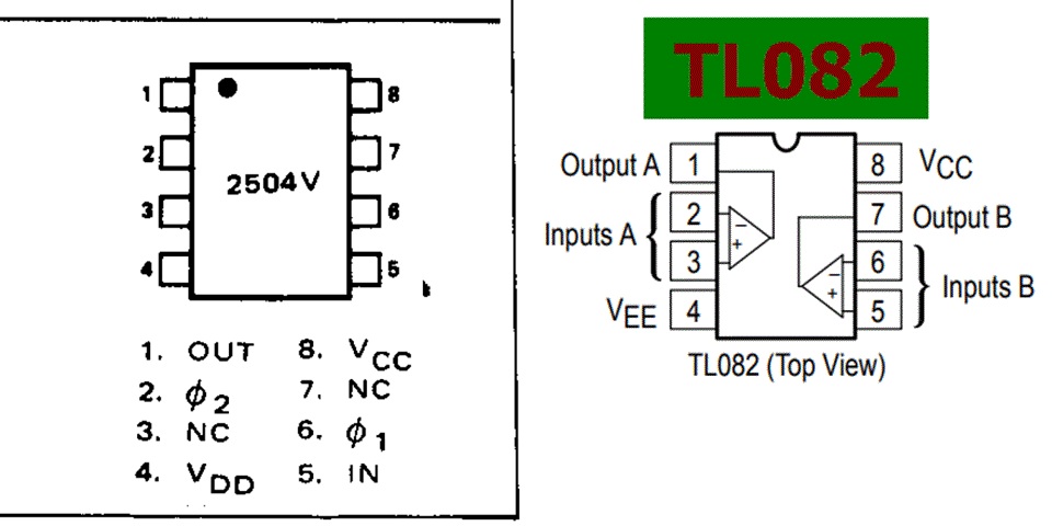
Pin 7 on the 2504V or AM1404 is not connected but on a dual op-amp that is the 2nd channel output pin. Sure enough, there is a signal on that pin which also resembles one of the clock inputs. So these supposed AM1404 APC ICs are definitely fake and almost certainly just dual op-amp ICs, virtually worthless. That puts the whole project in jeopardy as guaranteed genuine sources of these parts have become extremely scarce in recent times and the prices now possibly beyond my budget.
To be continued...
Apple computer model 1 (original) specifications
| Made | 1976 - 1977 |
| CPU | MOS Technology 6502 @ 1.023MHz (0.96 MHz including refresh waits) |
| RAM | 4 kByte expandable to 8 kByte on board |
| FDD | None |
| Ports | Optional Cassette interface, Expansion (44 way PCB edge connection) |
| O/S | Wozmon, Apple - 1 BASIC loaded via cassette. |
| Display | Monochrome, 40 x 24 characters displayed |
| Sound | None |
| Monitor | Monochrome Composite Video |
| Keyboard | Separate ASCII keyboard required. |
| Speakers | None |
Web Resources (External Links) -
Apple 1 Hardware Notes - willegal.net
Apple-1 replica gerber files - mi2k, applefritter.com
Updated 2519 replacement board - ebruchez, github.com
How the Apple 1 computer works. - The 8-Bit Guy, YouTube
More on Apple 1 -5 Volt Supply Issues and a Solution - willegal.net
How to fix the nonstandard Apple-1 video - UncleBernie, applefritter.com
All images and text on this website are Copyright.
Contact: jbtech at telstra dot com